

18F452 Datasheet – Flash Microcontroller (PIC18F452)
Enhanced Flash Microcontroller with 10-Bit A/D
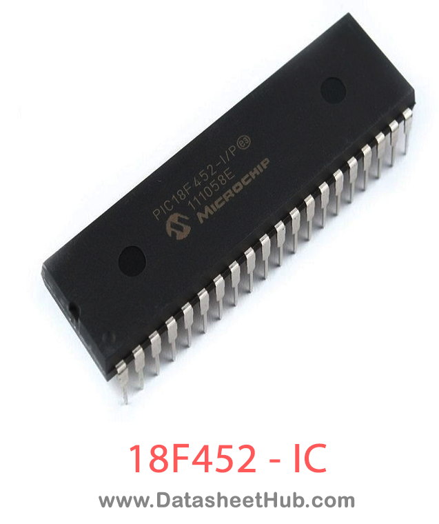
18F452 overview
The 18F452 is an Enhanced Flash Microcontroller with 10-Bit A/D made by Microchip Technology, supplied in these packages: PLCC, TQFP 44 Pin Type. The absolute maximum ratings table on this page lists the 14 limits from the manufacturer's datasheet that must not be exceeded. This page brings together the 18F452 pinout and maximum ratings, with the full datasheet PDF to preview below or download.
The 18F452 is an advanced microcontroller renowned for its versatile applications in modern electronics. With its robust capabilities and embedded features, the 18F452 serves as a cornerstone in various industries, from industrial automation to consumer electronics. Its adaptability, reliable performance, and seamless integration make it a pivotal component for developing innovative solutions. Whether in automotive systems, IoT devices, or control applications, the 18F452 embodies the essence of modern technology, contributing to the enhancement of electronic designs across diverse sectors.
These devices come in 28-pin and 40/44-pin packages. The 28-pin devices do not have a Parallel Slave Port (PSP) implemented and the number of Analog-to- Digital (A/D) converter input channels is reduced to 5.The following two figures are device block diagrams sorted by pin count: 28-pin for Figure 1-1 and 40/44-pin for Figure 1-2. The 28-pin and 40/44-pin pinouts are listed in Table 1-2 and Table 1-3, respectively.
Datasheet
18F452 features
- Peripheral Features
- High current sink/source 25 mA/25 mA
- Three external interrupt pins
- Timer0 module: 8-bit/16-bit timer/counter with 8-bit programmable prescaler
- Timer1 module: 16-bit timer/counter
- Timer2 module: 8-bit timer/counter with 8-bit period register (time-base for PWM)
- Timer3 module: 16-bit timer/counter
- Secondary oscillator clock option - Timer1/Timer3
- Capture input: capture is 16-bit, max. resolution 6.25 ns (TCY/16)
- Compare is 16-bit, max. resolution 100 ns (TCY)
- PWM output: PWM resolution is 1- to 10-bit, max. PWM freq. @: 8-bit resolution = 156 kHz 10-bit resolution = 39 kHz
- 3-wire SPI™ (supports all 4 SPI modes)
- I2C™ Master and Slave mode
- Addressable USART module: Supports RS-485 and RS-232
- Supports RS-485 and RS-232
- Parallel Slave Port (PSP) module
- Analog Features
- Fast sampling rate
- Conversion available during SLEEP
- Linearity £ 1 LSb
- Programmable Low Voltage Detection (PLVD) - Supports interrupt on-Low Voltage Detection
- - Supports interrupt on-Low Voltage Detection
- Programmable Brown-out Reset (BOR)
- Special Microcontroller Features
- 100,000 erase/write cycle Enhanced FLASH program memory typical
- 1,000,000 erase/write cycle Data EEPROM memory
- FLASH/Data EEPROM Retention: > 40 years
- Self-reprogrammable under software control
- Power-on Reset (POR), Power-up Timer (PWRT) and Oscillator Start-up Timer (OST)
- Watchdog Timer (WDT) with its own On-Chip RC Oscillator for reliable operation
- Programmable code protection
- Power saving SLEEP mode
- Selectable oscillator options including
- 4X Phase Lock Loop (of primary oscillator)
- Secondary Oscillator (32 kHz) clock input
- Single supply 5V In-Circuit Serial Programming™ (ICSP™) via two pins
- In-Circuit Debug (ICD) via two pins
18F452 pinout
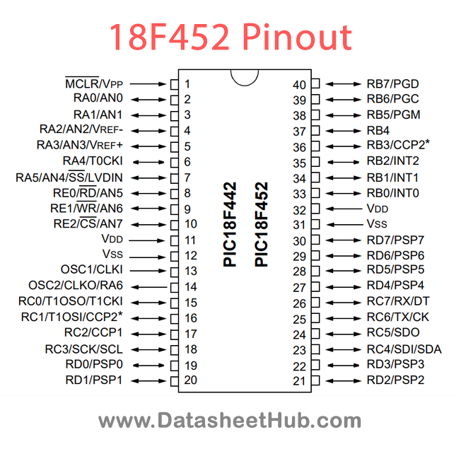
| Pin | Name | Description |
|---|---|---|
| SOIC | DIP | |
| 1 | MCLR/VPP MCLR VPP | ST ST |
| — | NC | — |
| 9 | OSC1/CLKI OSC1 CLKI | ST CMOS |
| 10 | OSC2/CLKO/RA6 OSC2 | — |
| CLKO | — | |
| RA6 | TTL | |
| 2 | RA0/AN0 | |
| RA0 | TTL | |
| AN0 | Analog | |
| 3 | RA1/AN1 | |
| RA1 | TTL | |
| AN1 | Analog | |
| 4 | RA2/AN2/VREF- | |
| RA2 | TTL | |
| AN2 | Analog | |
| VREF- | Analog | |
| 5 | RA3/AN3/VREF+ | |
| RA3 | TTL | |
| AN3 | Analog | |
| VREF+ | Analog | |
| 6 | RA4/T0CKI | |
| RA4 | ST/OD | |
| T0CKI | ST |
Show all 30 pins
| Pin | Name | Description |
|---|---|---|
| 7 | RA5/AN4/SS/LVDIN | |
| RA5 | TTL | |
| AN4 | Analog | |
| SS | ST | |
| LVDIN | Analog | |
| RA6 |
Absolute maximum ratings
| Parameter | Value |
|---|---|
| Ambient temperature under bias | -55°C to +125°C |
| Storage temperature | -65°C to +150°C |
| Voltage on any pin with respect to VSS (except VDD, MCLR, and RA4) | 0.3V to (VDD + 0.3V) |
| Total power dissipation | 1.0W |
| Maximum current out of VSS pin | 300 mA |
| Maximum current into VDD pin | 250 mA |
| Input clamp current, IIK (VI < 0 or VI > VDD) | ±20 mA |
| Output clamp current, IOK (VO < 0 or VO > VDD) | ±20 mA |
| Maximum output current sunk by any I/O pin. | 25 mA |
| Maximum output current sourced by any I/O pin | 25 mA |
| Maximum current sunk by PORTA, PORTB, and PORTE (Note 3) (combined) | 200 mA |
| Maximum current sourced by PORTA, PORTB, and PORTE (Note 3) (combined) | 200 mA |
| Maximum current sunk by PORTC and PORTD (Note 3) (combined) | 200 mA |
| Maximum current sourced by PORTC and PORTD (Note 3) (combined) | 200 mA |
18F452 applications
- Microcontroller Applications
- Embedded Systems
- Industrial Automation
- Consumer Electronics
Comments 0
Leave a comment