
5P49V5901 Datasheet PDF – Programmable Clock Generator
Power Programmable Clock Generator
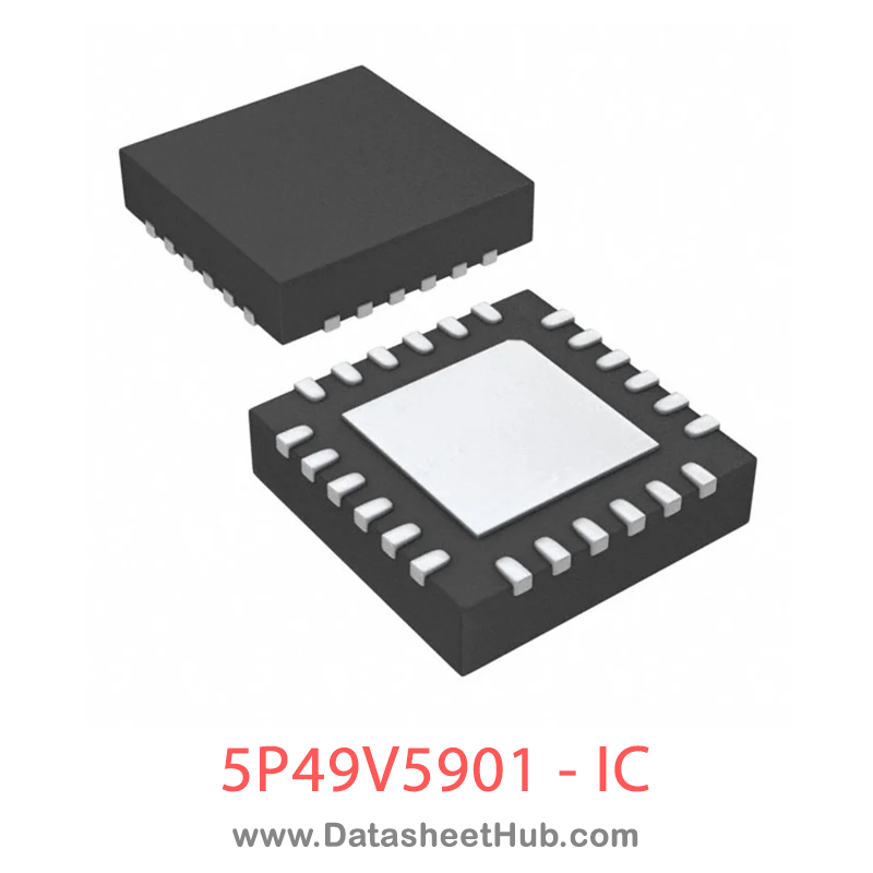
5P49V5901 overview
The 5P49V5901 is a Power Programmable Clock Generator, supplied in a 24-pin VFQFPN package. The absolute maximum ratings table on this page lists the 21 limits from the manufacturer's datasheet that must not be exceeded. This page brings together the 5P49V5901 pinout and maximum ratings, with the full datasheet PDF to preview below or download.
The 5P49V5901 is a programmable clock generator intended for high performance consumer, networking, industrial, computing, and data-communications applications.
Configurations may be stored in on-chip One-Time Programmable (OTP) memory or changed using I2C interface. This is IDTs fifth generation of programmable clock
The frequencies are generated from a single reference clock. The reference clock can come from one of the two redundant clock inputs. A glitchless manual switchover function allows one of the redundant clocks to be selected during normal operation.
Two select pins allow up to 4 different configurations to be programmed and accessible using processor GPIOs or bootstrapping. The different selections may be used for different operating modes (full function, partial function, partial power-down), regional standards (US, Japan, Europe) or system production margin testing. The device may be configured to use one of two I2C addresses to allow multiple devices to be used in a system
Datasheet
5P49V5901 features
- Generates up to four independent output frequencies
- Four fractional output dividers (FODs)
- Independent Spread Spectrum capability on each output pair
- Four banks of internal non-volatile in-system programmable or factory programmable OTP memory
- I2C serial programming interface
- One reference LVCMOS output clock
- Four universal output pairs: Each configurable as one differential output pair or two LVCMOS outputs
- Each configurable as one differential output pair or two LVCMOS outputs
- I/O Standards:Single-ended I/Os: 1.8V to 3.3V LVCMOS Differential I/Os - LVPECL, LVDS and HCSL
- Single-ended I/Os: 1.8V to 3.3V LVCMOS
- Differential I/Os - LVPECL, LVDS and HCSL
- Input frequency ranges
- LVCMOS Reference Clock Input (XIN/REF) – 1MHz to 200MHz
- LVDS, LVPECL, HCSL Differential Clock Input (CLKIN, CLKINB) – 1MHz to 350MHz
- Crystal frequency range: 8MHz to 40MHz
- Output frequency ranges: LVCMOS Clock Outputs – 1MHz to 200MHz
- LVCMOS Clock Outputs – 1MHz to 200MHz
- LVDS, LVPECL, HCSL Differential Clock Outputs – 1MHz to 350MHz
- Individually selectable output voltage (1.8V, 2.5V, 3.3V) for
- Redundant clock inputs with manual switchover
- Programmable loop bandwidth
- Programmable output to output skew
- Programmable slew rate control
- Programmable crystal load capacitance
- Individual output enable/disable
- Power-down mode
- 1.8V, 2.5V or 3.3V core VDDD, VDDA
- Available in 24-pin VFQFPN 4mm x 4mm package
- -40° to +85°C industrial temperature operation
5P49V5901 pinout
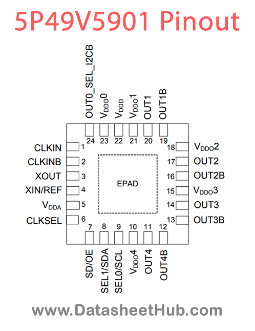
| Name | Description |
|---|---|
| CLKIN | Internal Pull-down |
| CLKINB | Internal Pull-down |
| XOUT | |
| XIN/REF | |
| VDDA | |
| CLKSEL | Internal Pull-down |
| SD/OE | Internal Pull-down |
| SEL1/SDA | Internal Pull-down |
| SEL0/SCL | Internal Pull-down |
| VDDO4 | |
| OUT4 | |
| OUT4B | |
| OUT3B | |
| OUT3 | |
| VDDO3 | |
| OUT2B | |
| OUT2 | |
| VDDO2 | |
| OUT1B | |
| OUT1 | |
| VDDO1 |
Absolute maximum ratings
| Parameter | Symbol | Value | Unit |
|---|---|---|---|
| Supply Voltage, VDDA, VDDD, VDDO | 3.465V | ||
| XIN/REF | 0V to 1.2V voltage swing | ||
| CLKIN, CLKINB | 0V to 1.2V voltage swing single-ended | ||
| Other inputs | -0.5V to VDDD | ||
| Outputs, VDDO (LVCMOS) | -0.5V to VDDO+ 0.5V | ||
| Outputs, IO (SDA) | 10mA | ||
| Package Thermal Impedance, qJA | 42°C/W (0 mps) | ||
| Package Thermal Impedance, qJC | 41.8°C/W (0 mps) | ||
| Storage Temperature, TSTG | -65°C to 150°C | ||
| ESD Human Body Model | 2000V | ||
| Junction Temperature | 125°C | ||
| Power supply voltage for supporting 1.8V outputs | VDDOX | Min 1.71 / Type 1.8 / Max 1.89 | V |
| Power supply voltage for supporting 2.5V outputs | VDDOX | Min 2.375 / Type 2.5 / Max 2.625 | V |
| Power supply voltage for supporting 3.3V outputs | VDDOX | Min 3.135 / Type 3.3 / Max 3.465 | V |
| Power supply voltage for core logic functions | VDDD | Min 1.71 / Max 3.465 | V |
| Analog power supply voltage. Use filtered analog power supply. | VDDA | Min 1.71 / Max 3.465 | V |
| Operating temperature, ambient | TA | Min -40 / Max +85 | °C |
| Maximum load capacitance (3.3V LVCMOS only) | CLOAD_OUT | Max 15 | pF |
| External reference crystal | FIN | Min 8 / Max 40 | MHz |
| 5 | External reference clock CLKIN, CLKINB | Type 350 | |
| Power up time for all VDDs to reach minimum specified voltage (power ramps must be monotonic) | tPU | Min 0.05 / Max 5 | ms |
5P49V5901 applications
- Ethernet switch/router
- PCI Express 1.0/2.0/3.0
- Broadcast video/audio timing
- Multi-function printer
Comments 0
Leave a comment