

74LS365 Hex Buffer with Logical OR Tri-State
Package PDIP, SOIC Series 74LS

74LS365 overview
The 74LS series of integrated circuits (ICs) was one of the most popular logic families of transistor-transistor logic (TTL) logic chips. 74LS series is a bipolar, low-power Schottky IC. 74LS365 Hex buffers and line drivers are designed specifically to improve both the performance and the density of three-state memory address drivers, clock drivers, and bus-oriented receivers and transmitters.

Key specifications
Supply Voltage
4.75 - 5.25Vdc
Maximum Clock Frequency
40Mhz
Power Dissipation
2mW/gate @100kHz
Minimum Output Current
8mA
Propagation Delay
10nS
Fan Out (TTL Loads)
20
Datasheet
365.pdf
74LS365 features
- Designed to Improve Performance and Density of Three-State Memory Address Drivers
- 3-State Outputs Drive Bus Lines
- Choice of True or Inverting Outputs
- Operating Temperature up to 70°C
- Standard TTL Switching Voltages
74LS365 pinout
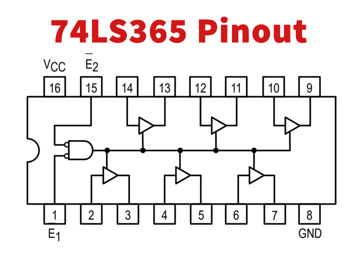
| Pin | Name | Description |
|---|---|---|
| 1 | E1 | Enable Pin |
| 2 | A1 | Input Of Buffer 1 |
| 3 | OUT 1 | Output Of Buffer 1 |
| 4 | A2 | Input Of Buffer 2 |
| 5 | OUT 2 | Output Of Buffer 2 |
| 6 | A3 | Input Of Buffer 3 |
| 7 | OUT 3 | Output Of Buffer 3 |
| 8 | GND | Ground |
| 9 | OUT 4 | Output Of Buffer 4 |
| 10 | A4 | Input Of Buffer 4 |
| 11 | OUT 5 | Output Of Buffer 5 |
| 12 | A5 | Input Of Buffer 5 |
| 13 | OUT 6 | Output Of Buffer 6 |
| 14 | A6 | Input Of Buffer 6 |
| 15 | E'2 | Enable Pin (Active Low) |
| 16 | VCC | Positive Supply |
74LS365 applications
- A buffered pH is a necessity of most enzymes to function efficiently and correctly. Furthermore, buffering is important for ensuring proper colour concentration when using dyes.
More about 74LS365
74LS365 Alternative Equivalent
74LS367, 74LS368
Comments 0
Leave a comment