
83940BY Datasheet – 8 LVPECL-to-LVCMOS/ LVTTL Fanout Buffer
Low Skew, 1-to-18 LVPECL-to LVCMOS/LVTTL Fanout Buffer / Eighteen LVCMOS/LVTTL outputs, 16Ωtypical output impedance

83940BY overview
The 83940BY is a Low Skew, 1-to-18 LVPECL-to LVCMOS/LVTTL Fanout Buffer / Eighteen LVCMOS/LVTTL outputs, 16Ωtypical output impedance, supplied in a 32-Lead LQFP Type package. The absolute maximum ratings table on this page lists the 5 limits from the manufacturer's datasheet that must not be exceeded. This page brings together the 83940BY pinout and maximum ratings, with the full datasheet PDF to preview below or download.
The ICS83940 is a low skew, 1-to-18 LVPECL- to-LVCMOS Fanout Buffer and a member of the HiPerClockS™ family of High Performance Clock Solutions from ICS. The ICS83940 has two selectable clock inputs. The PCLK, nPCLK pair can accept LVPECL, CML, or SSTL input levels. The LVCMOS_CLK can accept LVCMOS or LVTTL input levels. The low impedance LVCMOS outputs are designed to drive 50W series or parallel terminated transmission lines. The ICS83940 is characterized at full 3.3V, full 2.5V and mixed 3.3V input and 2.5V output operating supply modes. Guaran- teed output and part-to-part skew characteristics make the ICS83940 ideal for those clock distribution applications de- manding well defined performance and repeatability
Datasheet
83940BY features
- 18 LVCMOS outputs, 23W typical output impedance
- Selectable LVCMOS_CLK or LVPECL clock inputs
- PCLK, nPCLK supports the following input types: LVPECL, CML, SSTL
- LVCMOS_CLK accepts the following input levels: LVCMOS or LVTTL
- Maximum output frequency: 250MHz
- Output skew: 150ps (maximum)
- Part to part skew: 750ps (maximum)
- Full 3.3V or 2.5V supply modes
- 0°C to 70°C ambient operating temperature
- Industrial temperature information available upon request
- Pin compatible with the MPC940L
83940BY pinout
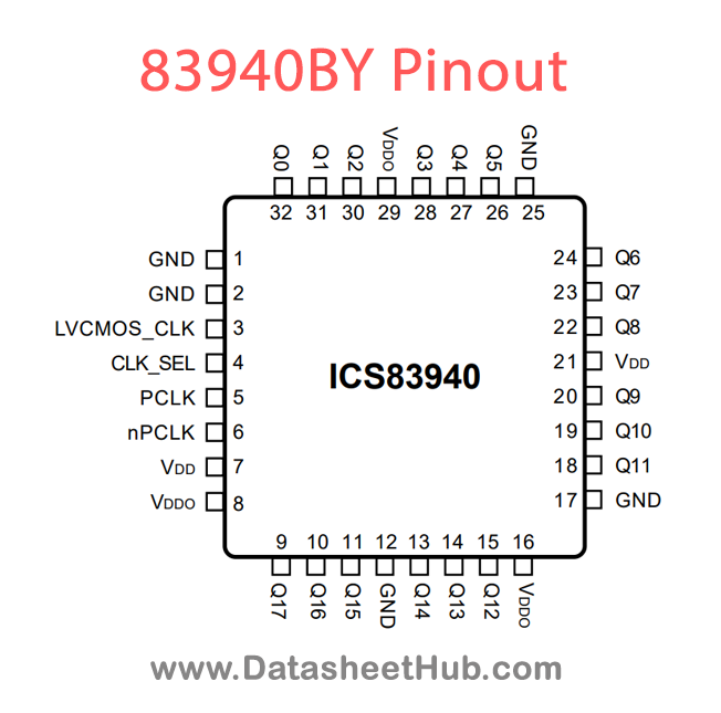
| Name | Description |
|---|---|
| GND | Power supply ground. |
| LVCMOS_CLK | Clock input. LVCMOS / LVTTL interface levels. |
| CLK_SEL | Clock select input. Selects LVCMOS / LVTTL clock input when HIGH. Selects PCLK, nPCLK inputs when LOW. LVCMOS / LVTTL interface levels. |
| PCLK | Non-inverting differential LVPECL clock input. |
| nPCLK | Inverting differential LVPECL clock input. |
| VDD | Positive supply pins. |
| VDDO | Output supply pins. |
| Q17, Q16, Q15, Q14, Q13, Q12, Q11, Q10, Q9, Q8, Q7, Q6, Q5, Q4, Q3, Q2, Q1, Q0 | Clock outputs. 23W typical output impedance. LVCMOS / LVTTL interface levels. |
Absolute maximum ratings
| Parameter | Value |
|---|---|
| Supply Voltage, VDDx | 4.6V |
| Inputs, VI | -0.5V to VDD + 0.5 V |
| Outputs, VO | -0.5V to VDDO + 0.5V |
| Package Thermal Impedance, qJA | 47.9°C/W (0 lfpm) |
| Storage Temperature, Tstg | -65°C to 150°C |
83940BY applications
- High-Speed Data Transmission
- Telecommunication Systems
- Optical Fiber Networks
- Data Centers
Comments 0
Leave a comment