

AM4379 Datasheet – Sitara Processor, Arm Cortex-A9
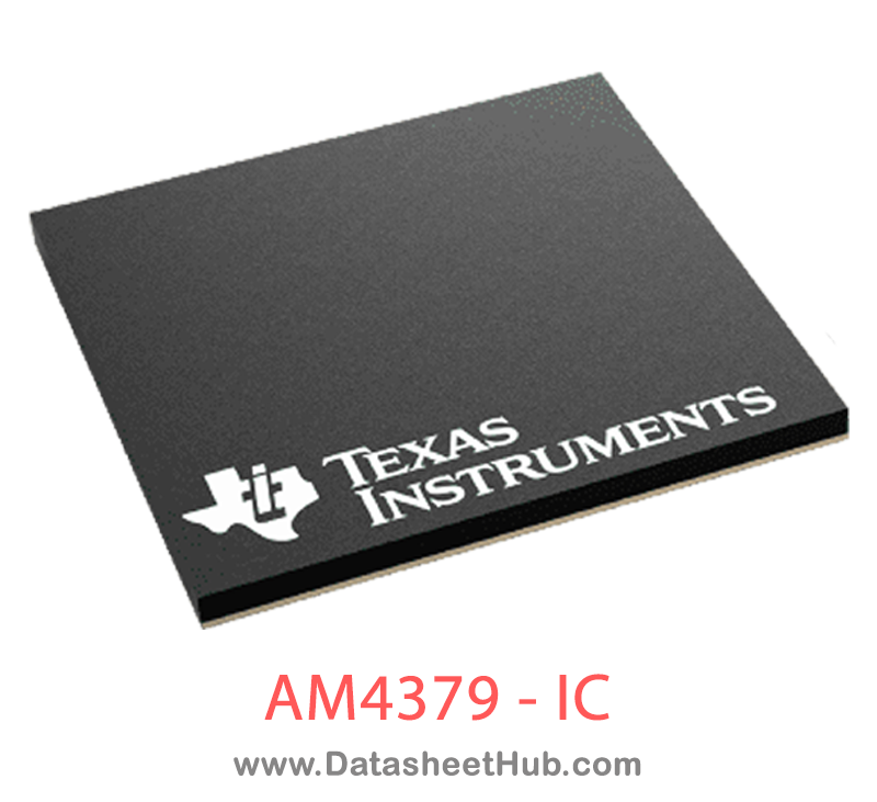
AM4379 overview
The AM4379 is a Sitara processor, Arm Cortex-A9 made by Texas Instruments, supplied in a 491 NFBGA Pin type package. The absolute maximum ratings table on this page lists the 40 limits from the manufacturer's datasheet that must not be exceeded. This page brings together the AM4379 maximum ratings, with the full datasheet PDF to preview below or download.
The TI AM437x high-performance processors are based on the ARM Cortex-A9 core.
The processors are enhanced with 3D graphics acceleration for rich graphical user interfaces, as well as a coprocessor for deterministic, real-time processing including industrial communication protocols, such as EtherCAT, PROFIBUS, EnDat, and others. The devices support high-level operating systems (HLOS). Linux® is available free of charge from TI. Other HLOSs are available from TI's Design Network and ecosystem partners.
These devices offer an upgrade to systems based on lower performance ARM cores and provide updated peripherals, including memory options such as QSPI-NOR and LPDDR2.
The processor subsystem is based on the ARM Cortex-A9 core, and the PowerVR SGX™ graphics accelerator subsystem provides 3D graphics acceleration to support display and advanced user interfaces.
The programmable real-time unit subsystem and industrial communication subsystem (PRU-ICSS) is separate from the ARM core and allows independent operation and clocking for greater efficiency and flexibility. The PRU-ICSS enables additional peripheral interfaces and real-time protocols such as EtherCAT, PROFINET, EtherNet/IP, PROFIBUS, Ethernet Powerlink, Sercos, EnDat, and others. The PRU-ICSS enables EnDat and another industrial communication protocol in parallel. Additionally, the programmable nature of the PRU-ICSS, along with their access to pins, events and all system-on-chip (SoC) resources, provides flexibility in implementing fast real-time responses, specialized data handling operations, custom peripheral interfaces, and in off-loading tasks from the other processor cores of the SoC.
High-performance interconnects provide high-bandwidth data transfers for multiple initiators to the internal and external memory controllers and to on-chip peripherals. The device also offers a comprehensive clock-management scheme.
One on-chip analog to digital converter (ADC0) can couple with the display subsystem to provide an integrated touch-screen solution. The other ADC (ADC1) can combine with the pulse width module to create a closed-loop motor control solution.
The RTC provides a clock reference on a separate power domain. The clock reference enables a battery- backed clock reference.
The camera interface offers configuration for a single- or dual-camera parallel port. Cryptographic acceleration is available in all devices. All other supported security features, including support for Secure boot, debug security and support for Trusted execution environment is available on HS (High-Security) devices. For more information about HS devices, contact your TI sales representative.
Datasheet
AM4379 features
- Highlights
- NEON™ SIMD Coprocessor and Vector Floating Point (VFPv3) Coprocessor
- 32KB of Both L1 Instruction and Data Cache
- 256KB of L2 Cache or L3 RAM
- 32-Bit LPDDR2, DDR3, and DDR3L Support
- General-Purpose Memory Support (NAND, NOR, SRAM) Supporting up to 16-Bit ECCSGX530 Graphics Engine
- Display Subsystem
- Programmable Real-Time Unit Subsystem and Industrial Communication Subsystem (PRU- ICSS) Real-Time Clock (RTC)
- Up to Two USB 2.0 High-Speed Dual-Role (Host or Device) Ports With Integrated PHY
- 10, 100, and 1000 Ethernet Switch Supporting up to Two Ports
- Serial Interfaces
- Two Controller Area Network (CAN) Ports
- Six UARTs, Two McASPs, Five McSPIs, Three I2C Ports, One QSPI, and One HDQ or 1-Wire
- Security
- Crypto Hardware Accelerators (AES, SHA, RNG, DES, and 3DES)
- Secure Boot (Avaliable Only on AM437x High-Security [AM437xHS] Devices)
- Two 12-Bit Successive Approximation Register (SAR) ADCs
- Up to Three 32-Bit Enhanced Capture (eCAP) Modules
- Up to Three Enhanced Quadrature Encoder Pulse (eQEP) Modules
- Up to Six Enhanced High-Resolution PWM (eHRPWM) Modules
- MPU Subsystem
- 64KB of On-Chip RAM
- Emulation and DebugJTAGEmbedded Trace Buffer
- JTAG
- Embedded Trace Buffer
- Interrupt Controller
- On-Chip Memory (Shared L3 RAM)
- 256KB of General-Purpose On-Chip Memory Controller (OCMC) RAM
- Accessible to All Masters
- Supports Retention for Fast Wakeup
- Up to 512KB of Total Internal RAM
- (256KB of ARM Memory Configured as L3 RAM
- + 256KB of OCMC RAM)
- External Memory Interfaces (EMIFs) DDR Controllers: LPDDR2: 266-MHz Clock (LPDDR2-533 Data Rate)
- DDR Controllers: LPDDR2: 266-MHz Clock (LPDDR2-533 Data Rate)
- LPDDR2: 266-MHz Clock (LPDDR2-533 Data Rate)
- DDR3 and DDR3L: 400-MHz Clock (DDR-
Absolute maximum ratings
| Parameter | Value | Unit |
|---|---|---|
| VDD_MPU | Min Supply voltage for the MPU domain / Max –0.5 | 1.5 |
| VDD_CORE | Min Supply voltage range for the CORE domain / Max –0.5 | 1.5 |
| CAP_VDD_RTC(3) | Min Supply voltage range for the RTC domain / Max –0.5 | 1.5 |
| VDDS_RTC | Min Supply voltage range for the RTC domain / Max –0.5 | 2.1 |
| VDDS_OSC | Min Supply voltage range for the System oscillator / Max –0.5 | 2.1 |
| VDDS_SRAM_CORE_BG | Min Supply voltage range for the Core SRAM and Bandgap LDOs / Max –0.5 | 2.1 |
| VDDS_SRAM_MPU_BB | Min Supply voltage range for the MPU SRAM and BB LDOs / Max –0.5 | 2.1 |
| VDDS_PLL_DDR | Min Supply voltage range for the DPLL DDR / Max –0.5 | 2.1 |
| VDDS_PLL_CORE_LCD | Min Supply voltage range for the DPLL CORE, EXTDEV, and LCD / Max –0.5 | 2.1 |
| VDDS_PLL_MPU | Min Supply voltage range for the DPLL MPU / Max –0.5 | 2.1 |
| VDDS_DDR | Min Supply voltage range for the DDR IO domain / Max –0.5 | 2.1 |
| VDDS | Min Supply voltage range for all dual-voltage IO domains / Max –0.5 | 2.1 |
| VDDA1P8V_USB0 | Min Supply voltage range for USBPHY and DPLL PER / Max –0.5 | 2.1 |
| VDDA1P8V_USB1 | Min Supply voltage range for USBPHY / Max –0.5 | 2.1 |
| VDDA_ADC0 | Min Supply voltage range for ADC0 / Max –0.5 | 2.1 |
| VDDA_ADC1 | Min Supply voltage range for ADC1 / Max –0.5 | 2.1 |
| VDDSHV1 | Min Supply voltage range for the dual-voltage IO domain / Max –0.5 | 3.8 |
| VDDSHV2 | Min Supply voltage range for the dual-voltage IO domain / Max –0.5 | 3.8 |
| VDDSHV3 | Min Supply voltage range for the dual-voltage IO domain / Max –0.5 | 3.8 |
| VDDSHV5 | Min Supply voltage range for the CLKOUT voltage domain / Max –0.5 | 3.8 |
| VDDSHV6 | Min Supply voltage range for the dual-voltage IO domain / Max –0.5 | 3.8 |
| VDDSHV7 | Min Supply voltage range for the dual-voltage IO domain / Max –0.5 | 3.8 |
| VDDSHV8 | Min Supply voltage range for the dual-voltage IO domain / Max –0.5 | 3.8 |
| VDDSHV9 | Min Supply voltage range for the dual-voltage IO domain / Max –0.5 | 3.8 |
| VDDSHV10 | Min Supply voltage range for the dual-voltage IO domain / Max –0.5 | 3.8 |
| VDDSHV11 | Min Supply voltage range for the dual-voltage IO domain / Max –0.5 | 3.8 |
| VDDA3P3V_USB0 | Min Supply voltage range for USBPHY / Max –0.5 | 4 |
| VDDA3P3V_USB1 | Min Supply voltage range for USBPHY / Max –0.5 | 4 |
| VDDS3P3V_IOLDO | Min Supply voltage range for the dual-voltage IO LDO / Max –0.5 | 3.8 |
| VDDS_CLKOUT | Min Supply voltage range for CLKOUT domain / Max –0.5 | 2.1 |
| USB0_VBUS(4) | Min Supply voltage range for USB VBUS comparator input / Max –0.5 | 5.25 |
| USB1_VBUS(4) | Min Supply voltage range for USB VBUS comparator input / Max –0.5 | 5.25 |
| DDR_VREF | Min Supply voltage range for the DDR3/DDR3L HSTL, LPDDR2 HSUL_12 reference voltage / Max –0.3 | 1.1 |
| Steady State Max. Voltage at all IO pins (5) | Max –0.5 V to IO supply voltage + 0.3 V | |
| USB0_ID(6) | Min Steady state maximum voltage range for the USB ID input / Max –0.5 | 2.1 |
| USB1_ID(6) | Min Steady state maximum voltage range for the USB ID input / Max –0.5 | 2.1 |
| Transient Overshoot and Undershoot specification at IO terminal | Max 20% of corresponding IO supply voltage for up to 20% of signal period | |
| Latch-up Performance | Min Class II (105°C) / Max Latch-up I-test performance current-pulse injection on each IO pin | ±100 |
| Latch-up overvoltage performance voltage injection on each IO pin | Min ±100 | |
| Tstg | Min Storage temperature / Max –55 | 155 |
AM4379 applications
- Patient Monitoring
- Navigation Equipment
- Industrial Automation
- Portable Data Terminals
- Bar Code Scanners
- Point of Service
- Portable Mobile Radios
- Test and Measurement
Comments 0
Leave a comment