

BQ24737 Datasheet – Battery SMBus Charge Controller

BQ24737 overview
The BQ24737 is a Battery SMBus Charge Controller made by Texas Instruments, supplied in a QFN-20 Type package. The absolute maximum ratings table on this page lists the 7 limits from the manufacturer's datasheet that must not be exceeded. This page brings together the BQ24737 pinout and maximum ratings, with the full datasheet PDF to preview below or download.
The bq24725 is a high-efficiency, synchronous battery charger, offering low component count for space-constraint, multi-chemistry battery charging applications. The bq24725 uses two charge pumps to separately drive n-channel MOSFETs (ACFET, RBFET and BATFET) for automatic system power source selection SMBus controlled input current, charge current, and charge voltage DACs allow for high regulation accuracies that can be programmed by the system power management micro-controller The bq24725 uses internal input current register or external ILIM pin to throttle down PWM modulation to reduce the charge current The bq24725 charges two, three or four series Li+ cells, and is available in a 20-pin, 3.5 x 3.5 mm2 QFN Package
Datasheet
BQ24737 features
- SMBus Host-Controlled NMOS-NMOS Synchronous Buck Converter with Programmable 615kHz, 750kHz, and 885kHz Switching Frequencies
- Automatic N-channel MOSFET Selection of System Power Source from Adapter or Battery Driven by Internal Charge Pumps
- Enhanced Safety Features for Over Voltage .
- Protection, Over Current Protection, Battery,
- Inductor and MOSFET Short Circuit Protection
- Programmable Input Current, Charge Voltage,
- Charge Current Limits .
- ±0.5% Charge Voltage Accuracy up to 19.2V
- ±3% Charge Current Accuracy up to 8.128A
- ±3% Input Current Accuracy up to 8.064A
- ±2% 20x Adapter Current or Charge Current Amplifier Output Accuracy
BQ24737 pinout
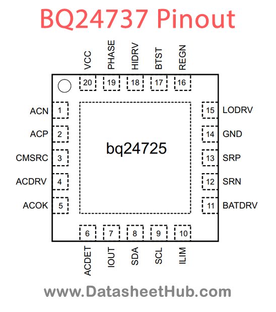
| Pin | Name | Description |
|---|---|---|
| 1 | ACN | Input current sense resistor negative input. Place an optional 0.1 µF ceramic capacitor from ACN to GND for common- mode filtering. Place a 0.1µF ceramic capacitor from ACN to ACP to provide differential mode filtering. |
| 2 | ACP | Input current sense resistor positive input. Place a 0.1µF ceramic capacitor from ACP to GND for common-mode filtering. Place a 0.1 µF ceramic capacitor from ACN to ACP to provide differential-mode filtering. |
| 3 | CMSRC | ACDRV charge pump source input. Place a 4kΩ resistor from CMSRC to the common source of ACFET (Q1) and RBFET (Q2) limit the in-rush current on the CMSRC pin. |
| 4 | ACDRV | Charge pump output to drive both adapter input n-channel MOSFET (ACFET) and reverse blocking n-channel MOSFET (RBFET). ACDRV voltage is 6V above CMSRC when voltage on ACDET pin is between 2.4V to 3.15V, voltage on VCC pin is above UVLO and voltage on VCC pin is 275mV above voltage on SRN pin so that |
| 5 | ACOK | AC adapter detection open drain output. It is pulled HIGH to external pull-up supply rail by external pull-up resistor when voltage on ACDET pin is between 2.4V and 3.15V, and voltage on VCC is above UVLO and voltage on VCC pin is 275mV above voltage on SRN pin, indicating a valid adapter is present |
| 6 | ACDET | Adapter detection input. Program adapter valid input threshold by connecting a resistor divider from adapter input to ACDET pin to GND pin. When ACDET pin is above 0.6V and VCC is above UVLO, REGN LDO is present, ACOK comparator and IOUT are both active. |
| 7 | IOUT | Buffered adapter or charge current output, selectable with SMBus command Charge Option(). IOUT voltage is 20 times the differential voltage across sense resistor. Place a 100pF or less ceramic decoupling capacitor from IOUT pin to GND. |
| 8 | SDA | SMBus open-drain data I/O. Connect to SMBus data line from the host controller or smart battery. Connect a 10kΩ pull- up resistor according to SMBus specifications. |
| 9 | SCL | SMBus open-drain clock input. Connect to SMBus clock line from the host controller or smart battery. Connect a 10kΩ pull-up resistor according to SMBus specifications. |
| 10 | ILIM | Charge current limit input. Program ILIM voltage by connecting a resistor divider from system reference 3.3V rail to ILIM pin to GND pin. The lower of ILIM voltage or DAC limit voltage sets charge current regulation limit. To disable the control on ILIM, set ILIM above 1.6V. Once voltage on ILIM pin |
| 11 | BATDRV | Charge pump output to drive Battery to System n-channel MOSFET (BATFET). BATDRV voltage is 6V above SRN to turn on BATFET (Q5) to power the system from battery. BATDRV voltage is SRN voltage to turn off BATFET to power system from AC adapter. Place a 4kΩ resistor from BATDRV to the gate of BATFET li |
| 12 | SRN | Charge current sense resistor negative input. SRN pin is for battery voltage sensing as well. Connect the SRN pin to a 7.5Ω resistor first then from resistor another terminal connect a 0.1µF ceramic capacitor to GND for common-mode filtering and connect to current sensing resistor. Connect a 0.1µF c |
Absolute maximum ratings
| Parameter | Value | Unit |
|---|---|---|
| Voltage range | SRN, SRP, ACN, ACP, CMSRC, VCC | –0.3 to 30 |
| PHASE | –2 to 30 | |
| ACDET, SDA, SCL, LODRV, REGN, IOUT, ILIM, ACOK | –0.3 to 7 | |
| BTST, HIDRV, ACDRV, BATDRV | –0.3 to 36 | |
| Maximum difference voltage | SRP–SRN, ACP–ACN | –0.5 to 0.5 |
| Junction temperature range, TJ | –40 to 155 | °C |
| Storage temperature range, Tstg | –55 to 155 | °C |
BQ24737 applications
- Portable Notebook Computers, UMPC, Ultra- Thin Notebook, and Netbook
- Personal Digital Assistant
- Handheld Terminal
- Industrial and Medical Equipment
- Portable Equipment
Comments 0
Leave a comment