

CM501 Datasheet – PMIC for LCD TV / Monitor
LCD driver for Sharp LC-42SV50U
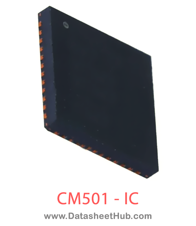
CM501 overview
The CM501 is an LCD driver for Sharp LC-42SV50U made by RichTek Technology, supplied in a QFN48 Type package. The absolute maximum ratings table on this page lists the 21 limits from the manufacturer's datasheet that must not be exceeded. This page brings together the CM501 pinout and maximum ratings.
The CM501 generates all the supply rails for thin-film transistor (TFT) liquid-crystal display (LCD) panels in TVs and Monitors. It includes boost and buck regulators, VGH and VGL charge pump regulators, gate pulse modulator (GPM) , HV LDO, voltage detector (XAO) and VCOM OP. The CM501 can support input voltage from 8V to 14V and is optimized for LCD TV panel and LCD monitor applications running directly from 12V supply.
The boost and buck regulators feature internal power MOSFETs and high-frequency operation allowing the use of small inductors and capacitors, resulting in a compact solution. Both switching regulators use fixed-frequency, current-mode control architectures, providing fast load- transient response and easy compensation.
The VGH and VGL charge-pump regulators provide supply voltages for TFT gate driver. Both output voltages can be adjusted with external resistive voltage dividers.
The GPM is controlled by frame signals from timing controller to modulate the Gate-On voltage (VGHM), which acts as a flicker compensation to reduce the coupling effect between gate lines and pixels. It also can delay VGHM while power-on for achieving a correct power-on sequence for gate driver ICs. VGHM power-on delay time, the falling time and falling stop voltage can be programmable by an external capacitor and an external resistor.
The voltage detector (XAO) monitors VIN voltage to issue a reset signal while the detected voltage is too low. The detecting level is decided by an external resistive voltage divider.
The HV LDO can provide a highly accurate voltage (0.5%) for gamma reference voltage. It has fast transient response and also wide operation input range.
The VCOM OP can drive the LCD VCOM voltage that features high short-circuit current (300mA), fast slew rate (45V/ms), wide bandwidth (20MHz) and rail-to-rail inputs and outputs. The CM501 is available in a small WQFN-48L 7x7 package and operates over the -40°C to +85°C temperature range.
Datasheet
CM501 features
- 8V to 14V Supply Input Voltage Range
- Current-Mode Boost Regulator
- 20V 3.5A 0.1W Internal N-MOSFET
- Programmable Over Current Protection Voltage
- ±1% Accurate Output
- Programmable Soft-start
- Line Regulation 0.15%/V
- Load Regulation ±1%/A
- External Compensation
- Current-Mode Buck Regulator
- 16.5V 3.2A 0.15W Internal N-MOSFET
- Over Current Protection
- Adjustable Output Voltage from 1.8V to 3.3V
- Line Regulation 0.1%/V
- Load Regulation ±0.5%/A
- Internal Compensation
- Internal Soft-start
- Adjustable VGH Charge Pump ±2% Accurate Output Continuous Output Current 50mA
- ±2% Accurate Output
- Continuous Output Current 50mA
- Adjustable VGL Charge Pump
- Accurate Output Controlled by ( REF- FBN )
- Gate Pulse Modulator
- 18V to 35V Positive Supply Input
- Flicker Compensation
- Power-On/Off Sequence Control
- On-Chip GPM Controller with Adjustable Falling Time and Falling Stop Voltage
- Voltage Detector (XAO) Adjustable Detecting Voltage (±1%) N-Channel Open-Drain Output
- Adjustable Detecting Voltage (±1%)
- N-Channel Open-Drain Output
- VCOM OP
- 5V to 20V Input Supply Voltage
- ±300mA Output Short-Circuit Current for 1ms
- 45V/ms Slew Rate
- 20MHz, -3dB Bandwidth
- Rail-to-Rail Input/Output
- HVLDO
CM501 pinout

| Pin | Name | Description |
|---|---|---|
| 1 | VREF_I | Linear Regulator Input. Bypass VREF_I to GND with a 1mF capacitor close to the pin. |
| 2 | VOP | Operational Amplifier Supply Input. Connect this pin to the output of boost regulator and bypass to OPGND with a 1mF capacitor. |
| 3 | OGND | Ground for Operational Amplifiers. Connect this pin to power ground underneath the IC. |
| 4 | OPP | Operational Amplifier Non-Inverting Input. |
| 5 | OPN | Operational Amplifier Inverting Input. |
| 6 | OPO | Operational Amplifier Output. |
| 7 | XAO | Reset Function Output. |
| 8 | GVOFF | High-Voltage Switch Control Input. When GVOFF is high, the high voltage switch between VGH and VGHM is on and the high-voltage switch between VGHM and DRN is off. When GVOFF is low, the switch between VGH and VGHM is off and the switch between VGHM and DRN is on. GVOFF is inhibited by the VIN under- |
| 9 | EN | Enable Input. Pulling EN high enables boost regulator and VGH charge pump. |
| 10 | FB2 | Buck Regulator Feedback Input. Connect FB2 to the center of a resistive voltage-divider between buck regulator output and GND to set buck regulator output voltage. |
| 11 | OUT | Buck Regulator Output Sense Input. OUT is the inverting input to the internal current-sense amplifier. Connect OUT directly to the step-down regulator output. |
| 12 | GND2 | Buck Regulator Power Ground. |
| 13,14 | LX2 | Buck Regulator Switching Node. LX2 is the source of the internal high-side MOSFET. Connect the inductor and Schottky catch diode to LX2 and minimize the trace area for low EMI performance. |
| 15 | BST | Buck Regulator Bootstrap Pin. BST is the supply for the high-side MOSFET gate driver. Connect a 0.1μF ceramic capacitor from BST to LX2. |
| 16,17 | IN2 | Buck Regulator Supply Input. |
| 18 | GND | Analog Ground. |
| 19 | VDET | Voltage Detection Input. Connect VDET to the center of a resistive voltage-divider between VIN and AGND. |
| 20 | INVL | 4V Internal Linear Regulator and Startup Circuitry Supply Input. The input voltage range of INVL is between +8V and +14V. Connect a 1mF ceramic capacitor between INVL and GND. Place the capacitor close to the IC. |
| 21 | NC | No Internal Connection. |
| 22 | FSEL | Frequency Select Pin. Connect FSEL to VIN or leaving FSEL unconnected for 750kHz operation. Connect this pin to GND for 500kHz operation. |
| 23 | CLIM | Boost Regulator OCP level setting by an external resistor to GND. |
| 24 | SS | Soft-Start Control Pin. Connect a soft-start capacitor (CSS) to this pin. Soft-start capacitor is charged with 5mA. The soft start capacitor is discharged to ground when EN is low. If CSS is less than 200pF, soft-start is controlled internally and soft-start time is 10ms. Otherwise, the soft-start t |
| 25,26 | LX1 | Boost Regulator Switching Node. Connect the inductor and the Schottky diode to LX1 and minimize the trace area for low EMI. |
| 27,28 | PGND | Boost Regulator Power Ground. |
Absolute maximum ratings
| Parameter | Value |
|---|---|
| IN2, INVL, SUPN, FSEL to GND | -0.3V to 16.5V |
| SUPP, GD_I, VOP, VREF_I to GND | -0.3V to 20V |
| VOP to GND | -0.3V to 20V |
| DRVP tO CPGND | -0.3V to (VSUPP + 0.3V) |
| DRVN to GND | -0.3V to (VSUPN + 0.3V) |
| OPO, OPP, OPN to OGND | -0.3V to (VVOP + 0.3V) |
| VREF_O to GND | -0.3V to (VVREF_I + 0.3V) |
| l FB1, FB2, FBP, FBN, GVOFF, DLY1, VREF_FB, THR, EN to GND | -0.3V to 6.5V |
| l OUT, VL, REF, COMP, SS, XAO, VDEV, CLIM to GND | -0.3V to 6.5V |
| GD2, OPGND, CPGND to GND | ±0.3V |
| BST to GND2 | -0.3V to 20V |
| LX1 to PGND | -0.3V to 20V |
| LX2 to GND2 | -0.3V to (IN2+0.3V) |
| VGHM, VGH, DRN to GND | -0.3V to 40V |
| VGH to VGHM | -0.3V to 40V |
| VGH, VGHM to DRN | -0.3V to 40V |
| Power Dissipation, PD @ TA = 25°C WQFN-48L 7x7 | 2.941W |
| Package Thermal Resistance (Note 3) WQFN-48L 7x7, qJAWQFN-48L 7x7, qJC | 34°C/W7°C/W |
| Junction Temperature | 150°C |
| Lead Temperature (Soldering, 10 sec.) | 260°C |
| Storage Temperature Range | -65°C to 150°C |
CM501 applications
- LCD TV / Monitor
- Home Security
- Industrial Monitoring
- Environmental Control
- Healthcare Devices
Comments 0
Leave a comment