
GL800USB Datasheet PDF – USB2.0 UTMI Transceiver IC
3.3 V, USB 2.0 UTMI Compliant Transceiver

GL800USB overview
The GL800USB is a 3.3 V, USB 2.0 UTMI Compliant Transceiver made by Genesys Logic, supplied in an LQFP 48 pin Type package. The absolute maximum ratings table on this page lists the 7 limits from the manufacturer's datasheet that must not be exceeded. This page brings together the GL800USB pinout and maximum ratings, with the full datasheet PDF to preview below or download.
GL800USB is a high performance USB 2.0 Transceiver compliant with the UTMI (USB 2.0 Transceiver Macrocell Interface) Specification proposed by Intel. The UTMI specification defines a standard interface to USB 2.0 high-speed transceivers that enables common design across prototype and production implementations.
The GL800USB integrates high-speed, mixed-signal circuitry to serve as the interface between the high performance USB serial bus and the 16-bit SIE bus. The transceiver is controlled by input signals from the SIE bus, which is synchronized with the 30MHz clock output. The UTMI transceiver handles the low level USB protocol and signaling. This includes features such as: data serialization and deserialization, bit stuffing and clock recovery and synchronization. The primary focus of the UTMI transceiver is to shift the clock domain of the data from the USB 2.0 rate to one that is compatible with the general logic.
To eliminate the difficult high-speed, mixed-signal USB 2.0 logic design for system and peripheral developers, the GL800USB with standard UTMI and 40X improvement in data rate can be easily adapted for implementation of USB 2.0 high speed compliant design of widely applications, including scanners, printers, portable storage, external CD-ROM / CD-RW / DVD-ROM, flash card readers, and PC cameras.
Datasheet
GL800USB features
- Complies with Universal Serial Bus Specification Rev. 2.0.
- Complies with USB 2.0 Transceiver Macrocell Interface (UTMI) Specification.
- Supports 480 Mbit/s "High Speed" (HS) / 12 Mbit/s “Full Speed” (FS), FS Only serial data transmission rates.
- 16 bit Bi-directional Serial Interface Engine (SIE) bus
- SYNC/EOP generation and checking
- Supports “Chirp” for High Speed recognition
- Data and clock recovery from serial stream on the USB
- Bit-stuffing/unstuffing; bit stuff error detection
- Holding registers to stage transmit and receive data
- Supports Reset and Suspend
- Supports USB 2.0 Test Mode
- Single parallel data clock output with on-chip PLL to generate higher speed serial data clocks
- Available in 48 pin LQFP package (9 mm * 9mm)
GL800USB pinout
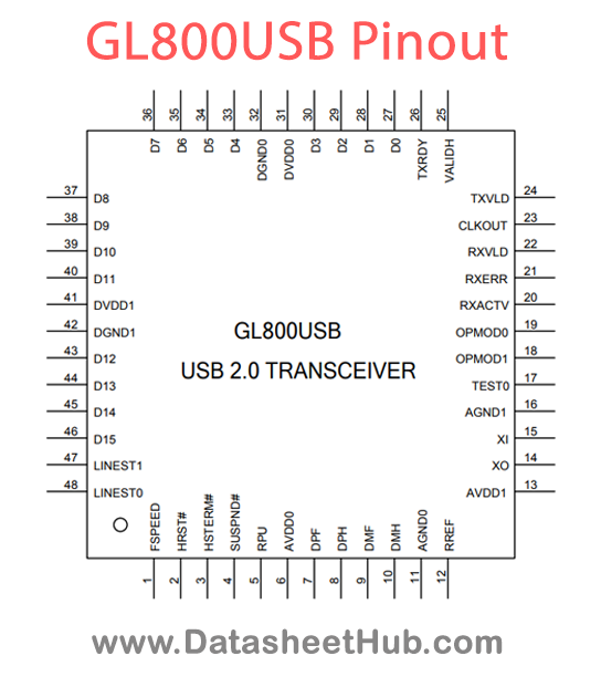
| Pin | Name | Description |
|---|---|---|
| 1 | FSPEED | Transceiver Select. This signal selects between the FS and HS transceivers: 0: High Speed transceiver enabled 1: Full Speed transceiver enabled |
| 2 | HRST# | Reset. Chip reset Input, active low. This signal is used to reset all state machines in the GL800USB. |
| 3 | HSTERM# | Termination Select. HS termination enable, active low |
| 4 | SUSPND# | Suspend mode enable, active low. This signal places the GL800USB in a mode that draws minimal power from supplies. Shuts down all blocks not necessary for Suspend/Resume operation. While suspended, HSTERM# must always be disabled (FS Mode) to ensure that the 1.5K pull-up on DP remains powered. |
| 5 | RPU | 3.3V Pull up control for DPF |
| 6 | AVCC0 | Positive analog supply (3.3V) |
| 7 | DPF | Positive USB differential data (Full Speed) |
| 8 | DPH | Positive USB differential data (High Speed) |
| 9 | DMF | Negative USB Differential Data (Full Speed) |
| 10 | DMH | Negative USB Differential Data (High Speed) |
| 11 | AGND0 | Analog ground (0V) |
| 12 | RREF | 510Ohm reference resistor input |
| 13 | AVCC1 | Positive analog supply (3.3V) |
| 14 | XO | Crystal output |
| 15 | XI | 12MHz crystal/oscillator input |
| 16 | AGND1 | Analog ground (0V) |
| 17 | TEST0 | Test mode enable |
| 18 | OPMOD1 | Operational mode. These signals select between various operational modes: [1] [0] Description 0 0 0: Normal Operation 1 1: Non-Driving0 2: Disable Bit Stuffing and NRZI encoding 1 1 3: Reserved |
| 19 | OPMOD0 |
Absolute maximum ratings
| Parameter | Symbol | Value |
|---|---|---|
| DC supply voltage | VCC | Min -0.5V / Max +3.6V |
| DC input voltage | VI | Min -0.5V / Max VCC+0.5V |
| DC input voltage range for I/O | VI/O | Min -0.5V / Max VCC+0.5V |
| DC input voltage for USB D+/D- pins | VAI/O | Min -0.5V / Max VCC+0.5V |
| DC voltage applied to outputs in High Z state | VI/OZ | Min -0.5V / Max VCC+0.5V |
| Static discharge voltage | VESD | Min 4000V |
| Ambient Temperature | TA | Min 0 oC / Max 100 oC |
GL800USB applications
- USB Hubs
- Embedded Systems
- Industrial Automation
- Medical Devices
Comments 0
Leave a comment