
H27UBG8T2CTR Datasheet – 32Gb MLC NAND Flash
32Gb(4096M x 8bit) Legacy MLC NAND Flash Memory
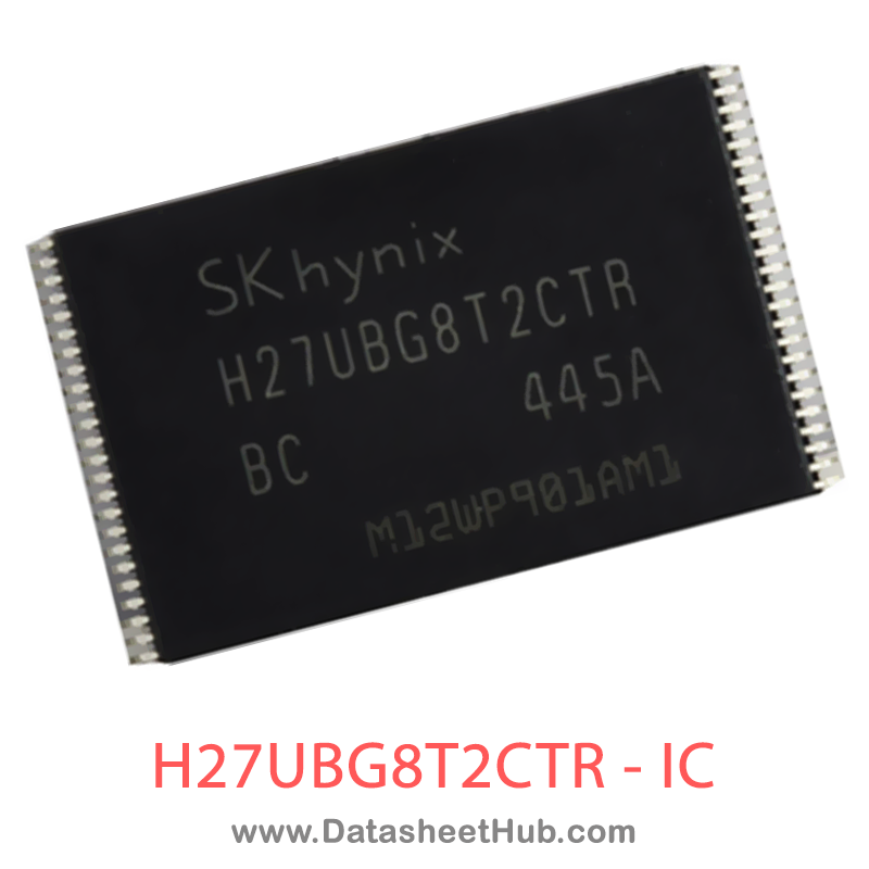
H27UBG8T2CTR overview
The H27UBG8T2CTR is a 32Gb(4096M x 8bit) Legacy MLC NAND Flash Memory, supplied in a TSOP-48/SDP Type package. The absolute maximum ratings table on this page lists the 7 limits from the manufacturer's datasheet that must not be exceeded. This page brings together the H27UBG8T2CTR pinout and maximum ratings, with the full datasheet PDF to preview below or download.
The product part NO.H27UBG8T2CTR-BC is a single 3.3V 32Gbit NAND flash memory. The Device contains 2 planes in a single die. Each plane is made up of the 1,044 blocks. Each block consists of 256 programmable pages. Each page contains 8,832 bytes. The pages are subdivided into an 8,192 byte main data storage area with a spare 640 byte district. Page program operation can be performed in typical 1,500us, and a single block can be erased in typical 5ms
Datasheet
H27UBG8T2CTR features
- Multi Level Cell (MLC) Technology
- NAND Interface
- x8 bus width
- Multiplexed address/data
- Pin-out compatibility for all densities
- Supply Voltage - Vcc = 2.7 V ~ 3.6 V
- - Vcc = 2.7 V ~ 3.6 V
- Organization
- Page size : 8832 (8192+640spare) bytes
- Block size : 256 pages (2M+160K) bytes
- Plane size : 1024 + 22 blocks
- Device size : 2048 + 44 Blocks
- Page Read Time Random Read Time(tR) : 60us / 80 us (Typ. / Max.) Sequential Access(tRC/tWC) : 16ns (Min.)
- Random Read Time(tR) : 60us / 80 us (Typ. / Max.)
- Sequential Access(tRC/tWC) : 16ns (Min.)
- Write Time Page program : 1500us (Typ.)
- Page program : 1500us (Typ.)
- Block Erase Time Block erase : 5ms (Typ.)
- Block erase : 5ms (Typ.)
- Multi-Plane Architecture
- Two independent planes architecture
- Parallel operations on both planes available, effectively halving program, read and erase time
- Command Set ONFI 1.0 Compliant Command Set Interleaved Copyback Program Read Unique IDs
- ONFI 1.0 Compliant Command Set
- Interleaved Copyback Program
- Read Unique IDs
- Package
- Package type : TSOP
- Chip count : SDP(1CE, Single) = 1stack
- Pin Count : 48
- Size : 12mm x 20mm x 1.2mm
- Electronic Signature
- 1st cycle : Manufacturer code
- 2nd cycle : Device code
- 3rd cycle : Internal chip number, Cell type, Number of simultaneously programmed pages
- 4th cycle : Page size, Block size, Organization, Spare size
- 5th cycle : Multi-plane information
- 6th cycle : Technology, EDO, Interface
- Hardware Data Protection Program/Erase locked during Power transitions
- Program/Erase locked during Power transitions
H27UBG8T2CTR pinout

| Name | Description |
|---|---|
| I/O 0― I/O 7 | DATA INPUTS/OUTPUTS The I/O pins is used to COMMAND LATCH cycle, ADDRESS INPUT cycle, and DATA in-out cycles during read / write operations. The I/O pins float to High-Z when the device is deselected or the outputs are disabled. |
| CLE | COMMAND LATCH ENABLE This input activates the latching of the I/O inputs inside the Command Register on the Rising edge of Write Enable (WE#). |
| ALE | ADDRESS LATCH ENABLE This input activates the latching of the I/O inputs inside the Address Register on the Rising edge of Write Enable (WE#). |
| CE# | CHIP ENABLE This input controls the selection of the device. When the device is busy, CE# low does not deselect the memory. The device goes into Stand-by mode when CE# goes High during the device is in Ready state. The CE# signal is ignored when device is in Busy state, and will not enter Standby mo |
| WE# | WRITE ENABLE This input acts as clock to latch Command, Address and Data. The I/O inputs are latched on the rise edge of WE#. |
| RE# | READ ENABLE The RE# input is the serial data-out control, and when active drives the data onto the I/O bus. Data is valid tREA after the falling edge of RE# which also increments the internal column address counter by one. |
| WP# | WRITE PROTECT The WP# pin, when Low, provides a hardware protection against undesired write operations. Hardware Write Protection is activated when the Write Protect pin is low. In this condition modify operation do not start and the content of the memory is not altered. Write Protect pin is not lat |
| R/B# | READY / BUSY The Ready/Busy output is an Open Drain pin that signals the state of the memory. |
| VCC | SUPPLY VOLTAGE The VCC supplies the power for all the operations. (Read, Write, and Erase). |
| VSS | GROUND |
| NC | NO CONNECTED |
Absolute maximum ratings
| Parameter | Symbol | Value | Unit |
|---|---|---|---|
| Ambient Operating Temperature (Commercial Temperature Range) | TA | 0 to 70 | ℃ |
| -25 to 85 | Ambient Operating Temperature (Extended Temperature Range) | ℃ | |
| -40 to 85 | Ambient Operating Temperature (Industrial Temperature Range) | ℃ | |
| Temperature Under Bias | TBIAS | -50 to 125 | ℃ |
| Storage Temperature | TSTG | -65 to 150 | ℃ |
| Input or Output Voltage | VIO | -0.6 to 4.6 | V |
| Supply Voltage | VCC | -0.6 to 4.6 | V |
H27UBG8T2CTR applications
- IoT (Internet of Things) Devices
- Wearable Technology
- Gaming Consoles
- Smart TVs
- Memory Expansion
Comments 0
Leave a comment