

LC78626E Datasheet – Digital Signal Processor IC
Digital Signal Processor for Compact Disc Player
LC78626E overview
The LC78626E is a monolithic compact disk player signal processing and servo control CMOS IC equipped with an internal anti-shock control function. Designed for total functionality including support for EFM-PLL, one-bit D/A converter, and containing an analog low-pass filter, the LC78626E provides optimal cost-performance for low-end CD players that provide anti-shock systems.
The basic functions provided by this IC include modulation of the EFM signal from the optical pick-up, deinterleaving, detection, and correction of signal errors, prevention of a maximum of approximately 10 seconds of skipping, signal processing such as digital filtering (which is useful in reducing the cost of the player), and processing of a variety of servo-related commands from the microprocessor.
| Part Number | LC78626E |
| Function | Digital Signal Processor for Compact Disc Player |
| Package | QIP100E, FLP100 Type |
| Manufacturer | SANYO (Panasonic) |
| Datasheet | Download PDF  |
Datasheet
LC78626E features
- 100-pin QFP
- A single 3.2 V/5 V power supply
- When an HF signal is input, it is sliced to precise levels and converted to an EFM signal. The phase is compared with the internal VCO and a PLL clock is reproduced at an average frequency of 4.3218 MHz.
- Precise timing for a variety of required internal timing needs (including the generation of the reference clock) is produced by the attachment of an external 16.9344 MHz crystal oscillator.
- The speed of revolution of the disk motor is controlled by the frame phase difference signal generated by the playback clock and the reference clock.
LC78626E pinout
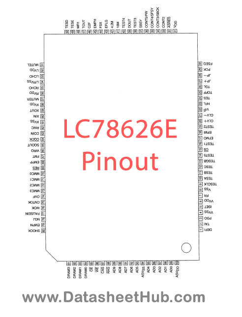
| Pin | Name | Description |
|---|---|---|
| 1 | DEFI | Defect detection signal (DEF) input. When not used, must be connected to 0 V. |
| 2 | TAI | For the PLL |
| 3 | PDO | External VCO control phase comparator output. |
| 4 | VVSS | Internal VCO ground. Must be connected to 0 V. |
| 5 | ISET | PDO output current adjustment resistor connection. |
| 6 | VVDD | Internal VCO power supply. |
| 7 | FR | VCO frequency range adjustment |
| 8 | VSS | Digital system ground. Must be connected to 0 V. |
| 9 | TESCLK | Test clock input. Must be connected to VDD. |
| 10 | TESA | Test operation mode control input. Must be connected to VDD. |
| 11 | TESB | Test operation mode control input. Must be connected to VDD. |
| 12 | TESC | Test operation mode control input. Must be connected to VDD. |
| 13 | TESGB | Test operation mode control input. Must be connected to VDD. |
| 14 | TEST5 | Chip select input. Equipped with an internal pull-down resistor. When not controlled, must be connected to 0 V. |
| 15 | CS | For slice-level control. |
| 16 | TEST1 | Test input. Must be connected to 0 V. |
| 17 | EFMO | Test input. Equipped with an internal pull-down resistor. Must be connected to 0 V. |
| 18 | EFMI | EFM signal input. |
| 19 | TEST2 | Sync signal detects output. A high level when the sync signal detected from the EFM signal matches the internally generated sync signal. |
| 20 | CLV+ | Disk motor control output. Can have a 3-state output depending on the command. |
| 21 | CLV– | |
| 22 | V/P | Rough servo/phase control automatic switching monitor output. If a high level then rough servo mode. If a low level then phase control mode. |
| 23 | HFL | Track detect signal input. Schmidt input. |
| 24 | TES | Tracking error signal input. Schmidt input. |
Show all 33 pins
| Pin | Name | Description |
|---|---|---|
| 25 | TOFF | Tracking off output. |
| 26 | TGL | Tracking gain switch output. Gain is increased with low level. |
| 27 | JP+ | Track jump control output. Can be 3-state output depending on the command. |
| 28 | JP– | |
| 29 | PCK | EFM data playback clock monitor. 4.3218 MHz during phase lock. |
| 30 | FSEQ | Sync signal detect output. A high level when the sync signal detected from the EFM signal matches the internally generated sync signal. |
| 31 | VDD | Digital system power supply. |
| 32 | ASRES | Reset signal input for initializing only the anti-shock control part (i.e. excluding the DSP part). Resets when this pin is low level, and release the reset when this pin is high level. Tie this pin to the low level (i.e., connected to 0 V) if when using software control on the anti-shock part alone |
| 33 | CONT2 | General I/O pin 2. This controls the commands from the microcontroller. When not used, either set this as an input port and connect to 0 V, or set this as an output port and leave it open. |
Absolute maximum ratings
| Parameter | Symbol | Value | Unit |
|---|---|---|---|
| Maximum power supply voltage | VDD max | VSS–0.3 to VSS+7.0 | V |
| Input voltage | VIN | VSS–0.3 to VDD+0.3 | V |
| Output voltage | VOUT | VSS–0.3 to VDD+0.3 | V |
| Allowable power dissipation | Pd max | 400 | mW |
| Operating temperature range | Topr | –20 to +75 | °C |
| Storage temperature range | Tstg | –40 to +125 | °C |
LC78626E applications
- Audio processing IC
- Digital sound controller
- Home entertainment systems
- Hi-fi audio devices
More about LC78626E
Pin Definitions
| Pin No. | Pin Name | I/O | Description | |
|---|---|---|---|---|
| 2 | TAI | I | For the PLL | Test input. Equipped with internal pull-down resistor. Must be connected to 0V. |
| 17 | EFMO | O | Test input. Equipped with an internal pull-down resistor. Must be connected to 0 V. | EFM signal output. |
| 32 | ASRES | I(I/O) | Reset signal input for initializing only the anti-shock control part (i.e. excluding the DSP part). Resets when this pin is low level, and release the reset when this pin is high level. Tie this pin to the low level (i.e., connected to 0 V) if when using software control on the anti-shock part alone through the anti-shock part only reset disable/release command ($F4) or the anti-shock only reset enable/inrush command ($F5). Note: This pin is assigned as the least significant bit of the general I/O port however, use as a general I/O pin is disabled. When the port I/O set command ($DB) is executed, the least significant bit is always “0,” and the output driver is not turned ON. | |
| Pin No. | Pin Name | I/O | Description | |
|---|---|---|---|---|
| 34 | CONT3/SBCK | I/O | General I/O pin 3. This controls the commands from the microcontroller. This pin is shared exclusively with the subcode read clock input (SBCK). When not used, either set this as an input port and connect to 0 V, or set this as an output port and leave it open. | |
| 35 | CONT4/SFSY | I/O | General I/O pin 4. This controls the commands from the microcontroller. This pin is shared exclusively with the subcode frame sync signal output (SFSY). When not used, either set this as an input port and connect to 0 V, or set this as an output port and leave it open. | |
| 36 | CONT5/PW | I/O | General I/O pin 5. This controls the commands from the microcontroller. This pin is shared, exclusively, with the subcode P, Q, R, S, T, U, V, W output (PW). When not used, either set this as an input port and connect to 0 V, or set this as an output port and leave it open. | |
| 37 | SBSY | O | Subcode block sync signal output. | |
| 38 | TEST3 | I | Test input. Equipped with an internal pull-down resistor. Must be connected to 0 V. | |
| 39 | DOUT | O | Digital output. EIAJ format. | |
| 40 | TEST4 | I | Test input. Equipped with an internal pull-down resistor. Must be connected to 0 V. | |
| 41 | 16M | O | 16.9344 MHz output. | |
| 42 | 4.2M | O | 4.2336 MHz output. | |
| 43 | EFLG | O | DRAM switch: high: 1M, low : 4M | |
| 44 | FSX | O | 7.35 kHz sync signal output (frequency divided from the crystal oscillator). | |
| 45 | EMPH | O | Deemphasis monitor output. When high level, a deemphasis disk is being played back. | |
| 46 | C2F | O | C2 flag output. | |
| 47 | TOUT | O | Test output. Under normal operation, this should be left open. | |
| 48 | MR1 | I | Operating mode switch: high: shockproof, low: through. | |
| 49 | TESE | I | Test input. Must be connected to 0V. | |
| 50 | TESD | I | Test input. Must be connected to 0V. | |
| 51 | MUTESL | O | For the one-bit D/A converter | L channel mute output. |
| 52 | LVDD | P | L channel power supply. | |
| 53 | LCHO | AO | L channel output. | |
| 54 | L/RVSS | P | L/R channel ground. Must be connected to 0 V. | |
| 55 | RCHO | AO | R channel output. | |
| 56 | RVDD | P | R channel power supply. | |
| 57 | MUTER | O | R channel mute output. | |
| 58 | XVDD | P | Crystal oscillator power supply. | |
| 59 | XOUT | O | 16.9344 MHz crystal oscillator connection. | |
| 60 | XIN | I | ||
| 61 | XVSS | P | Crystal oscillator ground. Must be connected to 0 V. | |
| 62 | RWC | I | Read/write control input. Schmidt input. | |
| 63 | COIN | I | Microcontroller command input. | |
| 64 | CQCK | I | Input pin for the command input latch clock and the subcode readout clock. Schmitt input. | |
| 65 | SQOUT | O | Subcode Q output. | |
| 66 | WRQ | O | Subcode Q output standby output. | |
| 67 | FMT | I | Operating mode switch: high: shock proof, low: through. | |
| 68 | EMPP | O | DRAM empty (an RZP pulse is output when the DRAM is empty). | |
| 69 | RES | I | External reset input: low reset (all internal blocks are reinitialized). | |
| Pin No. | Pin Name | I/O | Description |
|---|---|---|---|
| 70 | MMC0 | O | Remaining DRAM output. |
| 71 | MMC1 | O | Remaining DRAM output. |
| 72 | MMC2 | O | Remaining DRAM output. |
| 73 | MMC3 | O | Remaining DRAM output. |
| 74 | OVF | O | DRAM write terminated. (An RZP pulse is output when there is an overflow or a shock.) |
| 75 | CNTOK | O | C2F shock detects pause signal input: low: pause shock detection. |
| 76 | WOK | I | DRAM write enable signal input: high: write enable. |
| 77 | PAUSE IN | I | Pause signal input: high: pause. |
| 78 | NGJ | O | C2F data contact point detection start signal: low ® high: detection start. |
| 79 | EMPN | O | Remaining DRAM alarm output: low: memory low. |
| 80 | SHOCK | I | C2F shock detect pause signal input: low: pause shock detection. |
| 81 | DRAM3 | I/O | DRAM data bus |
| 82 | DRAM2 | I/O | DRAM data bus |
| 83 | DRAM1 | I/O | DRAM data bus |
| 84 | DRAM0 | I/O | DRAM data bus |
| 85 | OE | O | DRAM control signal. |
| 86 | WE | O | DRAM control signal. |
| 87 | CAS | O | DRAM control signal. |
| 88 | RAS | O | DRAM control signal. |
| 89 | AD9 | O | DRAM address bus |
| 90 | AD8 | O | DRAM address bus |
| 91 | AD7 | O | DRAM address bus |
| 92 | AD6 | O | DRAM address bus |
| 93 | AD5 | O | DRAM address bus |
| 95 | AD4 | O | DRAM address bus |
| 96 | AD3 | O | DRAM address bus |
| 97 | AD2 | O | DRAM address bus |
| 98 | AD1 | O | DRAM address bus |
| 99 | AD0 | O | DRAM address bus |
Comments 0
Leave a comment