

LM25085 Datasheet – PFET Buck Switching Controller
42V Constant On-Time PFET Buck Switching Controller

LM25085 overview
The LM25085 is a 42V Constant On-Time PFET Buck Switching Controller made by Texas Instruments, supplied in these packages: VSSOP, WSON, HVSSOP 8 Pin Type. The absolute maximum ratings table on this page lists the 5 limits from the manufacturer's datasheet that must not be exceeded. This page brings together the LM25085 pinout and maximum ratings, with the full datasheet PDF to preview below or download.
The LM25085 is a high efficiency PFET switching regulator controller that can be used to quickly and easily develop a small, efficient buck regulator for a wide range of applications. This high voltage controller contains a PFET gate driver and a high voltage bias regulator which operates over a wide 4.5V to 42V input range. The constant on-time regulation principle requires no loop compensation, simplifies circuit implementation, and results in ultra-fast load transient response. The operating frequency remains nearly constant with line and load variations due to the inverse relationship between the input voltage and the on-time. The PFET architecture allows 100% duty cycle operation for a low dropout voltage. Either the RDS(ON) of the PFET or an external sense resistor can be used to sense current for over-current detection
Datasheet
LM25085 features
- LM25085-Q1 is an Automotive Grade product that is AEC-Q100 Grade 1 Qualified (-40°C to 125°C Operating Junction Temperature)
- Wide 4.5V to 42V Input Voltage Range
- Adjustable Current Limit Using RDS(ON) or a Current Sense Resistor
- Programmable Switching Frequency to 1MHz
- No Loop Compensation Required
- Ultra-Fast Transient Response
- Nearly Constant Operating Frequency with Line and Load Variations
- Adjustable Output Voltage from 1.25V
- Precision ±2% Feedback Reference
- Capable of 100% Duty Cycle Operation
- Internal Soft-Start Timer
- Integrated High Voltage Bias Regulator
- Thermal Shutdown
LM25085 pinout
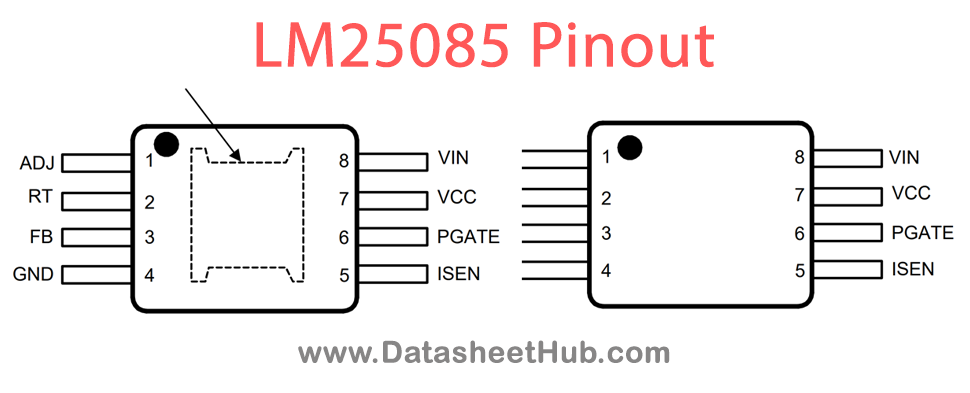
| Pin | Name | Description |
|---|---|---|
| 1 | ADJ | Current Limit Adjust - The current limit threshold is set by an external resistor from VIN to ADJ in conjunction with the external sense resistor or the PFET’s RDS(ON). |
| 2 | RT | On-time control and shutdown - An external resistor from VIN to RT sets the buck switch on-time and switching frequency. Grounding this pin shuts down the controller. |
| 3 | FB | Voltage Feedback from the regulated output - Input to the regulation and over-voltage comparators. The regulation level is 1.25V. |
| 4 | GND | Circuit Ground - Ground reference for all internal circuitry. |
| 5 | ISEN | Current sense input for current limit detection. Connect to the PFET drain when using RDS(ON) current sense. Connect to the PFET source and the sense resistor when using a current sense resistor. |
| 6 | PGATE | Gate Driver Output - Connect to the gate of the external PFET. |
| 7 | VCC | Output of the gate driver bias regulator - Output of the negative voltage regulator (relative to VIN) that biases the PFET gate driver. A low ESR capacitor is required from VIN to VCC, located as close as possible to the pins. |
| 8 | VIN | Input supply voltage - The operating input range is from 4.5V to 42V. A low ESR bypass capacitor must be located as close as possible to the VIN and GND pins. |
| EP | Exposed Pad - Exposed pad on the underside of the package (HVSSOP-PowerPAD-8 and WSON only). This pad is to be soldered to the PC board ground plane to aid in heat dissipation. |
Absolute maximum ratings
| Parameter | Value | Unit |
|---|---|---|
| VIN to GND | Min -0.3 / Max 45 | V |
| ISEN to GND | Min -3 / Max VIN + 0.3 | V |
| ADJ to GND | Min -0.3 / Max VIN + 0.3 | V |
| RT, FB to GND | Min -0.3 / Max 7 | V |
| VIN to VCC, VIN to PGATE | Min -0.3 / Max 10 | V |
LM25085 applications
- Automotive Infotainment
- Battery/Super Capacitor Chargers, LED Drivers
- DC-DC Buck Regulators
- Power Management
- Voltage Regulation
Comments 0
Leave a comment