

LTA803N Datasheet – LCD power management chip IC
LCD power management chip IC, PFC and flyback controller
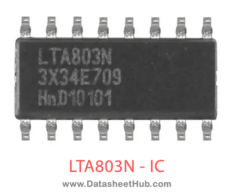
LTA803N overview
The LTA803N is an LCD power management chip IC, PFC and flyback controller made by Philips Electronics - NXP, supplied in an SOP 16 Pin package. The absolute maximum ratings table on this page lists the 22 limits from the manufacturer's datasheet that must not be exceeded. This page brings together the LTA803N pinout and maximum ratings, with the full datasheet PDF to preview below or download.
The TEA1753T is the third generation of green Switched Mode Power Supply (SMPS) controller ICs. The TEA1753T combines a controller for Power Factor Correction (PFC) and a flyback controller. Its high level of integration allows the design of a cost-effective power supply with a very low number of external components.
The special built-in green functions provide high efficiency at all power levels. This efficiency applies to quasi-resonant operation at high-power levels, quasi-resonant operation with valley skipping, as well as reduced frequency operation at lower power levels. At low-power levels, the PFC switches off to maintain high efficiency.
During low-power conditions, the flyback controller switches to frequency reduction mode and limits the peak current to an adjustable minimum value. This mode ensures high efficiency at low-power and good standby power performance while minimizing audible noise from the transformer.
The controller is switched to the power-down mode for no-load operation. In this mode, the controller is shut down for very low standby power applications.
The TEA1753T is a Multi-Chip Module, (MCM), containing two chips. The proprietary high-voltage BCD800 process which makes direct start-up possible from the rectified universal mains voltage in an effective and green way. The second low voltage Silicon On Insulator (SOI) is used for accurate, high-speed protection functions and control.
The TEA1753T enables the design of highly efficient and reliable supplies with power requirements of up to 250 W using the minimum number of external components.
Remark: All values provided throughout this data sheet are typical values unless otherwise stated.
Datasheet
LTA803N features
- Distinctive features
- Integrated PFC and flyback controller
- Universal mains supply operation (70 V (AC) to 276 V (AC))
- Dual-boost PFC with accurate maximum output voltage (NXP patented)
- High level of integration, resulting in a very low external component count and a cost-effective design
- Adjustable PFC switch off delay
- Green features
- On-chip start-up current source
- Power down functionality for very low standby power
- PFC green features
- Valley/Zero Voltage Switching (ZVS) for minimum switching losses (NXP patented)
- Frequency limitation to reduce switching losses
- PFC is switched off when a low load is detected at the flyback output
- Flyback green features
- Valley switching for minimum switching losses (NXP patented)
- Frequency reduction with adjustable minimum peak current at low-power operation to maintain high efficiency at low output power levels
- Protection features
- Safe restart mode for system fault conditions
- Continuous mode protection with demagnetization detection for both converters (NXP patented)
- Under Voltage Protection (UVP) (foldback during overload)
- Accurate Over Voltage Protection (OVP) for both converters (adjustable for flyback converter)
- Mains voltage independent Over Power Protection (OPP)
- Open control loop protection for both converters. The open-loop protection on the flyback converter is safe restart
- Over Temperature Protection (OTP)
- Low and adjustable Over Current Protection (OCP) trip level for both converters
- General-purpose latched protection input for system Over Temperature Protection (OTP) for example
LTA803N pinout
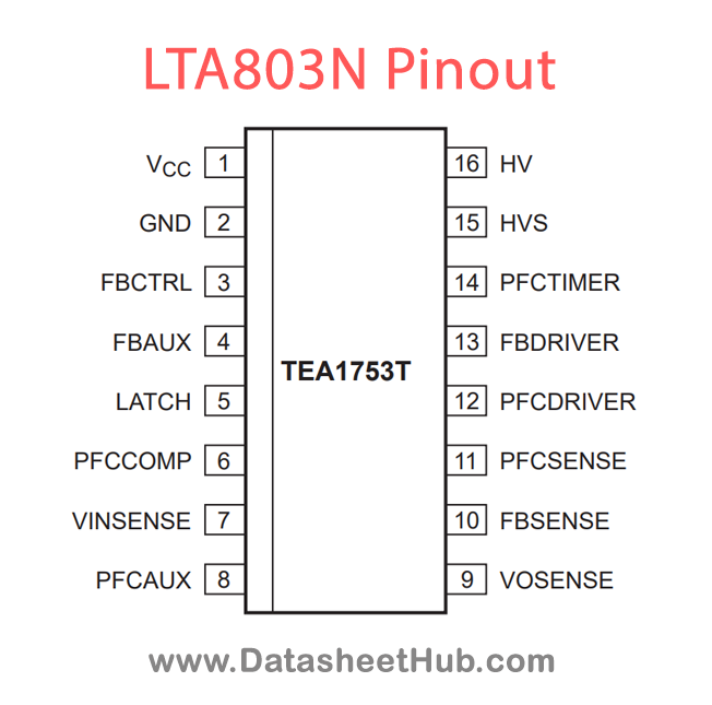
| Pin | Name | Description |
|---|---|---|
| 1 | VCC | supply voltage |
| 2 | GND | ground |
| 3 | FBCTRL | flyback control input |
| 4 | FBAUX | auxiliary winding input for demagnetization timing and flyback OVP |
| 5 | LATCH | general-purpose protection input |
| 6 | PFCCOMP | frequency compensation pin for PFC |
| 7 | VINSENSE | mains voltage sense input |
| 8 | PFCAUX | auxiliary winding input for demagnetization timing for PFC |
| 9 | VOSENSE | sense input for PFC output voltage |
| 10 | FBSENSE | flyback current sense input |
| 11 | PFCSENSE | PFC current sense input |
| 12 | PFCDRIVER | PFC gate-driver output |
| 13 | FBDRIVER | flyback gate-driver output |
| 14 | PFCTIMER | delay timer pin for PFC on/off control |
| 15 | HVS | high-voltage safety spacer, not connected |
| 16 | HV | high-voltage start-up / flyback valley sensing |
Absolute maximum ratings
| Parameter | Symbol | Value | Unit | Conditions |
|---|---|---|---|---|
| supply voltage | VCC | Min -0.4 / Max +38 | V | |
| voltage on the LATCH pin | VLATCH | Min -0.4 / Max +5 | V | current limited |
| voltage on the FBCTRL pin | VFBCTRL | Min -0.4 / Max +5 | V | |
| voltage on the PFCCOMP pin | VPFCCOMP | Min -0.4 / Max +5 | V | |
| voltage on the VINSENSE pin | VVINSENSE | Min -0.4 / Max +5 | V | |
| voltage on the VOSENSE pin | VVOSENSE | Min -0.4 / Max +5 | V | |
| voltage on the PFCAUX pin | VPFCAUX | Min -25 / Max +25 | V | |
| voltage on the FBSENSE pin | VFBSENSE | Min -0.4 / Max +5 | V | current limited |
| voltage on the PFCSENSE pin | VPFCSENSE | Min -0.4 / Max +5 | V | current limited |
| voltage on the PFCTIMER pin | VPFCTIMER | Min -0.4 / Max +5.5 | V | |
| voltage on the HV pin | VHV | Min -0.4 / Max +650 | V | |
| current on the FBCTRL pin | IFBCTRL | Min -3 / Max 0 | mA | |
| current on the FBAUX pin | IFBAUX | Min -1 / Max +1 | mA | |
| current on the PFCSENSE pin | IPFCSENSE | Min -1 / Max +10 | mA | |
| current on the FBSENSE pin | IFBSENSE | Min -1 / Max +10 | mA | |
| current on the FBDRIVER pin | IFBDRIVER | Min -0.8 / Max +2 | A | duty cycle < 10 % |
| current on the PFCDRIVER pin | IPFCDRIVER | Min -0.8 / Max +2 | A | duty cycle < 10 % |
| current on the HV pin | IHV | Max 8 | mA | |
| total power dissipation | Ptot | Max 0.6 | W | Tamb < 75 °C |
| storage temperature | Tstg | Min -55 / Max +150 | °C | |
| junction temperature | Tj | Min -40 / Max +150 | °C | |
| - | charged device | Min V | 500 |
LTA803N applications
- The device is used in all applications requiring an efficient and cost-effective power supply solutions up to 250 W. Notebook adapters in particular benefit from the high level of integration
Comments 0
Leave a comment