

MAX125 Datasheet – Simultaneous-Sampling 14-Bit DAS
2×4-Channel / Simultaneous-Sampling 14-Bit DAS
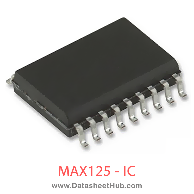
MAX125 overview
The MAX125 is a 2×4-Channel / Simultaneous-Sampling 14-Bit DAS made by Maxim Integrated, supplied in an SSOP 36 Pin Type package. The absolute maximum ratings table on this page lists the 6 limits from the manufacturer's datasheet that must not be exceeded. This page brings together the MAX125 pinout and maximum ratings, with the full datasheet PDF to preview below or download.
The MAX125/MAX126 are high-speed, multichannel, 14-bit data-acquisition systems (DAS) with simultaneous track/holds (T/Hs). These devices contain a 14-bit, 3µs, successive-approximation analog-to-digital converter (ADC), a +2.5V reference, a buffered reference input, and a bank of four simultaneous-sampling T/H amplifiers that preserve the relative phase information of the sampled inputs. The MAX125/MAX126 have two multiplexed inputs for each T/H, allowing a total of eight inputs. In addition, the converter is overvoltage tolerant to ±17V; a fault condition on any channel will not harm the IC. Available input ranges are ±5V (MAX125) and
±2.5V (MAX126). An on-board sequencer converts one to four channels per CONVST pulse. In the default mode, one T/H output (CH1A) is converted. An interrupt signal (INT) is provided after the last conversion is complete. Convert two, three, or four channels by reprogramming the MAX125/MAX126 through the bidirectional parallel interface. Once programmed, the MAX125/MAX126 continue to convert the specified number of channels per CONVST pulse until they are reprogrammed. The channels are converted sequentially, beginning with CH1. The INT signal always follows the end of the last conversion in a conversion sequence. The ADC converts each assigned channel in 3µs and stores the result in an internal 14x4 RAM. Upon completion of the conversions, data can be accessed by applying successive pulses to the RǍ pin. Four successive reads access four data words sequentially.
The parallel interface’s data-access and bus-release timing specifications are compatible with most popular digital signal processors and 16-bit/32-bit microprocessors, so the MAX125/MAX126 conversion results can be accessed without resorting to wait states.
Datasheet
MAX125 features
- Four Simultaneous-Sampling T/H Amplifiers with Two Multiplexed Inputs (eight single-ended inputs total)
- 3µs Conversion Time per Channel
- Throughput: 250ksps (1 channel) 142ksps (2 channels) 100ksps (3 channels) 76ksps (4 channels)
- 142ksps (2 channels)
- 100ksps (3 channels)
- 76ksps (4 channels)
- Input Range: ±5V (MAX125) ±2.5V (MAX126)
- ±2.5V (MAX126)
- Fault-Protected Input Multiplexer (±17V)
- ±5V Supplies
- Internal +2.5V or External Reference Operation
- Programmable On-Board Sequencer
- High-Speed Parallel DSP Interface
MAX125 pinout
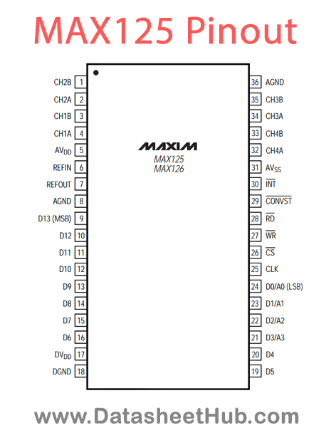
| Pin | Name | Description |
|---|---|---|
| 1, 2 | CH2B, CH2A | Channel 2 Multiplexed Inputs, single-ended |
| 3, 4 | CH1B, CH1A | Channel 1 Multiplexed Inputs, single-ended |
| 5 | AVDD | +5V ±5% Analog Supply Voltage |
| 6 | REFIN | External Reference Input/Internal Reference Output. Bypass with a 0.1µF capacitor to AGND. |
| 7 | REFOUT | Reference-Buffer Output. Bypass with a 4.7µF capacitor to AGND. |
| 8, 36 | AGND | Analog Ground. Both pins must be tied to ground. |
| 9–16 | D13–D6 | Data Bits. D13 = MSB. |
| 17 | DVDD | +5V ±5% Digital Supply Voltage |
| 18 | DGND | Digital Ground |
| 19, 20 | D5, D4 | Data Bits |
| 21–24 | D3/A3–D0/A0 | Bidirectional Data Bits/Address Bits. D0/A0 = LSB. |
| 25 | CLK | Clock Input (duty cycle must be 30% to 70%). |
| 26 | CS | Chip-Select Input (active-low) |
| 27 | WR | Write Input (active-low) |
| 28 | RǍ | Read Input (active-low) |
| 29 | CONVST | Conversion-Start Input. Rising edge initiates sampling and conversion sequence. |
| 30 | INT | Interrupt Output. Falling edge indicates the end of a conversion sequence. |
| 31 | AVSS | -5V ±5% Analog Supply Voltage |
| 32, 33 | CH4A, CH4B | Channel 4 Multiplexed Inputs, single-ended |
| 34, 35 | CH3A, CH3B | Channel 3 Multiplexed Inputs, single-ended |
Absolute maximum ratings
| Parameter | Value |
|---|---|
| CH_ _ to AGND | ±17V |
| Digital Inputs/Outputs to DGND | 0.3V to (DVDD + 0.3V) |
| Continuous Power Dissipation (TA = +70°C) SSOP (derate 11.8mW/°C above +70°C) | 941mW |
| Operating Temperature RangesMAX125CCAX/MAX126CCAXMAX125CEAX/MAX126CEAX | 0°C to +70°C -40°C to +85°C |
| Storage Temperature Range | -65°C to +150°C |
| Lead Temperature (soldering, 10sec). | 300°C |
MAX125 applications
- Multiphase Motor Control
- Power-Grid Synchronization
- Power-Factor Monitoring
- Digital Signal Processing
- Vibration and Waveform Analysis
Comments 0
Leave a comment