

MC74AC175 Datasheet – Quad D Flip-Flop With Master Reset
MC74AC175 overview
The MC74AC175 is a Quad D Flip-Flop With Master Reset made by Motorola, supplied in a DIP 16 Pin Type package. The absolute maximum ratings table on this page lists the 7 limits from the manufacturer's datasheet that must not be exceeded. This page brings together the MC74AC175 pinout and maximum ratings, with the full datasheet PDF to preview below or download.
The MC74AC/ACT175 is a high-speed quad D flip-flop. The device is useful for general flip-flop requirements where clock and clear inputs are common. The information on the D inputs is transferred to storage during the LOW-to-HIGH clock transition. The device has a Master Reset to simultaneously clear all flip-flops, when MR is low.
The MC74AC/ACT175 consists of four edge-triggered D flip-flops with individual D inputs and Q and Q outputs. The Clock (CP) and Master Reset (MR) are common to all flip-flops. Each D input’s state is transferred to the corresponding flip-flop’s output following the LOW-to-HIGH Clock (CP) transition. A LOW input to the Master Reset (MR) will force all Q outputs LOW and Q outputs HIGH independent of Clock or Data inputs. The MC74AC/ACT175 is useful for applications where the Clock and Master Reset are common to all storage elements.
Datasheet
MC74AC175 features
- Quad Flip-Flop: Contains four integrated flip-flops in one package.
- Data Enable Input: Offers control over data transfer with an external signal.
- High-Speed Operation: Known for its fast switching speeds.
- TTL-Compatible Inputs: Interfaces with both TTL and CMOS logic families.
- Outputs Source/Sink 24 mA
- ¢ACT175 Has TTL Compatible Inputs
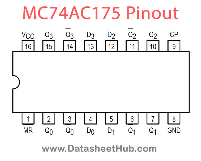
MC74AC175 pinout
| Name | Description |
|---|---|
| D0-D3 | Data input |
| Q0-Q3 | Outputs |
| Q0-Q3 | Outputs |
| CP | Clock Serial Input |
| MR | Master Reset Input |
Absolute maximum ratings
| Parameter | Symbol | Value | Unit |
|---|---|---|---|
| DC Supply Voltage (Referenced to GND) | VCC | –0.5 to +7.0 | V |
| DC Input Voltage (Referenced to GND) | Vin | –0.5 to VCC + 0.5 | V |
| DC Output Voltage (Referenced to GND) | Vout | –0.5 to VCC + 0.5 | V |
| DC Input Current, per Pin | Iin | ± 20 | mA |
| DC Output Sink/Source Current, per Pin | Iout | ± 50 | mA |
| DC VCC or GND Current per Output Pin | ICC | ± 50 | mA |
| Storage Temperature | Tstg | –65 to +150 | °C |
MC74AC175 applications
- Data Storage and Transfer Applications
- Shift Register Applications
- Counter Circuit Applications
- Frequency Division Applications
Comments 0
Leave a comment