

PIC16F877 Datasheet – 8-Bit CMOS FLASH Microcontroller
28/40-pin 8-Bit CMOS FLASH Microcontrollers

PIC16F877 overview
The PIC16F877 is a 28/40-pin 8-Bit CMOS FLASH Microcontrollers made by Microchip Technology, supplied in these packages: PLCC-3, QFP, DIP. The absolute maximum ratings table on this page lists the 14 limits from the manufacturer's datasheet that must not be exceeded. This page brings together the PIC16F877 pinout and maximum ratings, with the full datasheet PDF to preview below or download.
This document contains device specific information. Additional information may be found in the PIC® MCU Mid-Range Reference Manual (DS33023), which maybe obtained from your local Microchip Sales Representative or downloaded from the Microchip website. The Reference Manual should be considered a complementary document to this data sheet, and is highly recommended reading for a better understanding of the device architecture and operation of the peripheral modules.
There are four devices (PIC16F873, PIC16F874, PIC16F876 and PIC16F877) covered by this data sheet. The PIC16F876/873 devices come in 28-pin packages and the PIC16F877/874 devices come in 40-pin packages. The Parallel Slave Port is not implemented on the 28-pin devices. The following device block diagrams are sorted by pin number; 28-pin for Figure 1-1 and 40-pin for Figure 1-2. The 28-pin and 40-pin pinouts are listed in Table 1-1 and Table 1-2, respectively
Note 1: This buffer is a Schmitt Trigger input when configured as an external interrupt.
2: This buffer is a Schmitt Trigger input when used in Serial Programming mode.
3: This buffer is a Schmitt Trigger input when configured as general purpose I/O and a TTL input when used in the Parallel Slave Port mode (for interfacing to a microprocessor bus).
4: This buffer is a Schmitt Trigger input when configured in RC oscillator mode and a CMOS input otherwise.
3: This buffer is a Schmitt Trigger input when configured as general purpose I/O and a TTL input when used in the Parallel Slave Port mode (for interfacing to a microprocessor bus).4: This buffer is a Schmitt Trigger input when configured in RC oscillator mode and a CMOS input otherwise.
Datasheet
PIC16F877 features
- Microcontroller Core Features
- High performance RISC CPU
- Only 35 single word instructions to learn
- All single cycle instructions except for program branches which are two cycle
- Operating speed: DC - 20 MHz clock input DC - 200 ns instruction cycle
- DC - 20 MHz clock input
- DC - 200 ns instruction cycle
- Up to 8K x 14 words of FLASH Program Memory, Up to 368 x 8 bytes of Data Memory (RAM)
- Up to 256 x 8 bytes of EEPROM Data Memory
- Pinout compatible to the PIC16C73B/74B/76/77
- Interrupt capability (up to 14 sources)
- Eight level deep hardware stack
- Direct, indirect and relative addressing modes
- Power-on Reset (POR)
- Power-up Timer (PWRT) and Oscillator Start-up Timer (OST)
- Watchdog Timer (WDT) with its own on-chip RC oscillator for reliable operation
- Programmable code protection
- Power saving SLEEP mode
- Selectable oscillator options
- Low power, high speed CMOS FLASH/EEPROM technology
- Fully static design
- In-Circuit Serial Programmingä (ICSP) via two pins
- Single 5V In-Circuit Serial Programming capability
- In-Circuit Debugging via two pins
- Processor read/write access to program memory
- Wide operating voltage range: 2.0V to 5.5V
- High Sink/Source Current: 25 mA
- Commercial, Industrial and Extended temperature ranges
- Low-power consumption
- < 0.6 mA typical @ 3V, 4 MHz
- 20 mA typical @ 3V, 32 kHz
- < 1 mA typical standby current
- Peripheral Features
- Timer0: 8-bit timer/counter with 8-bit prescaler
- Timer1: 16-bit timer/counter with prescaler, can be incremented during SLEEP via external crystal/clock
- Timer2: 8-bit timer/counter with 8-bit period register, prescaler and postscaler
- Two Capture, Compare, PWM modules
- Capture is 16-bit, max. resolution is 12.5 ns
- Compare is 16-bit, max. resolution is 200 ns
- PWM max. resolution is 10-bit
PIC16F877 pinout
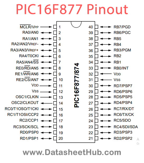
| Name | Description |
|---|---|
| OSC1/CLKIN | Oscillator crystal input/external clock source input. |
| OSC2/CLKOUT | Oscillator crystal output. Connects to crystal or resonator in crystal oscillator mode. In RC mode, the OSC2 pin outputs CLKOUT which has 1/4 the frequency of OSC1, and denotes the instruction cycle rate. |
| MCLR/VPP | Master Clear (Reset) input or programming voltage input. This pin is an active low RESET to the device. |
| RA0/AN0 | PORTA is a bi-directional I/O port. RA0 can also be analog input0. RA1 can also be analog input1. RA2 can also be analog input2 or negative analog reference voltage. RA3 can also be analog input3 or positive analog reference voltage. RA4 can also be the clock input to the Timer0 module. Output is op |
| RA1/AN1 | |
| RA2/AN2/VREF- | |
| RA3/AN3/VREF+ | |
| RA4/T0CKI | |
| RA5/SS/AN4 | |
| RB0/INT | PORTB is a bi-directional I/O port. PORTB can be software programmed for internal weak pull-up on all inputs. RB0 can also be the external interrupt pin. RB3 can also be the low voltage programming input. Interrupt-on-change pin. Interrupt-on-change pin. Interrupt-on-change pin or In-Circuit Debugge |
| RB1 | |
| RB2 | |
| RB3/PGM | |
| RB4 | |
| RB5 | |
| RB6/PGC | |
| RB7/PGD | |
| RC0/T1OSO/T1CKI | PORTC is a bi-directional I/O port. RC0 can also be the Timer1 oscillator output or Timer1 clock input. RC1 can also be the Timer1 oscillator input or Capture2 input/Compare2 output/PWM2 output. RC2 can also be the Capture1 input/Compare1 output/ PWM1 output. RC3 can also be the synchronous serial c |
| RC1/T1OSI/CCP2 | |
| RC2/CCP1 | |
| RC3/SCK/SCL | |
| RC4/SDI/SDA | |
| RC5/SDO | |
| RC6/TX/CK |
Show all 27 pins
| Name | Description |
|---|---|
| RC7/RX/DT | |
| VSS | Ground reference for logic and I/O pins. |
| VDD | Positive supply for logic and I/O pins. |
Absolute maximum ratings
| Parameter | Value |
|---|---|
| Ambient temperature under bias | -55 to +125°C |
| Storage temperature | -65°C to +150°C |
| Voltage on any pin with respect to VSS (except VDD, MCLR. and RA4) | 0.3 V to (VDD + 0.3 V) |
| Total power dissipation (Note 1) | 1.0 W |
| Maximum current out of VSS pin | 300 mA |
| Maximum current into VDD pin250 mA | 250 mA |
| Input clamp current, IIK (VI < 0 or VI > VDD) | ± 20 mA |
| Output clamp current, IOK (VO < 0 or VO > VDD) | ± 20 mA |
| Maximum output current sunk by any I/O pin | 25 mA |
| Maximum output current sourced by any I/O pin | 25 mA |
| Maximum current sunk by PORTA, PORTB, and PORTE (combined) (Note 3) | 200 mA |
| Maximum current sourced by PORTA, PORTB, and PORTE (combined) (Note 3) | 200 mA |
| Maximum current sunk by PORTC and PORTD (combined) (Note 3) | 200 mA |
| Maximum current sourced by PORTC and PORTD (combined) (Note 3) | 200 mA |
Comments 0
Leave a comment