
PL1167 Datasheet – Single Chip 2.4GHz Transceiver IC
Low Power High Performance Single Chip 2.4GHz Transceiver
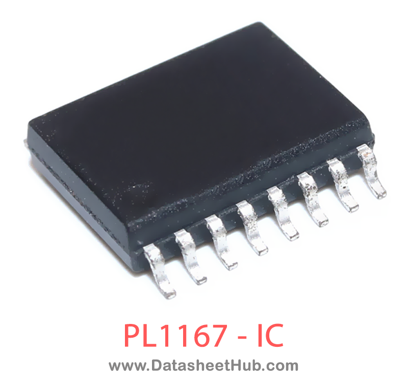
PL1167 overview
The PL1167 is a Low Power High Performance Single Chip 2.4GHz Transceiver, supplied in these packages: QFN16, SOP16 Type. The absolute maximum ratings table on this page lists the 6 limits from the manufacturer's datasheet that must not be exceeded. This page brings together the PL1167 pinout and maximum ratings, with the full datasheet PDF to preview below or download.
PL1167 is a piece of true low power high performance single chip 2.4GHz transceiver, which is designed for operation in the world wide ISM frequency band at 2.400~2.4835GHz. This single chip wireless transceiver integrated including: RF synthesizer, Power Amplifier, Crystal Oscillator, Modem and etc. All of the Output Power, Channel Selection, and Protocol can be configured through SPI Interface.
With built in FHSS and accurate digital RSSI, this transceiver achieves a good capability of anti-interference, so that, it can work under every complicated environment with high performance. It also support address and data check out; FEC, CRC function; and Auto-Ack & Auto-Resend function.
The output power of the chip can be set up to 2dBm and the receive sensitivity can achieve-88dBm. With on chip regulator and advanced power management function, the current consumption in sleep mode can be reduced to nearly 1uA
Datasheet
PL1167 features
- True Low Power High Performance Single Chip 2.4GHz Transceiver
- Built in Hardware Link Layer
- Built in Accurate Digital RSSI
- Support Auto-Ack and Auto-Resend Functions
- Built in Address and Data Checkout, FEC, CRC Functions
- Data Rate over the air:1Mbps
- Support SPI Bus Interface
- Support HFSS
- Support Micro-Strip Inductor and Two Layer PCB Boards
- 1.9 to 3.6V supply range
- Packages:QFN16/SOP16
PL1167 pinout
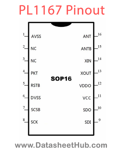
| Name | Description |
|---|---|
| 1 | RF |
| 2 | RF |
| 3, 8, 17 | Power |
| 4,5 | N/C |
| 6 | Digital Output |
| 7 | Digital Input |
| 9 | Digital Input |
| 10 | Digital Input |
| 11 | Digital Input |
| 12 | Digital Output |
| 13 | Power |
| 14 | Power |
| 15 | Analog Output |
| 16 | Analog Input |
Absolute maximum ratings
| Parameter | Symbol | Value | Unit |
|---|---|---|---|
| Supply Voltage of VCC | VCC | -0.3 to +3.6 | V |
| Supply Voltage of VDDO | VDDO | -0.3 to +2.5 | V |
| Input Voltage | VIN | -0.3 to (VCC+0.3) | V |
| Output Voltage | VOUT | -0.3 to (VCC+0.3) | |
| Operating Temperature | TOP | -40 to +85 | ℃ |
| Storage Temperature | TST | -40 to +125 | ℃ |
PL1167 applications
- Wireless Sensor Networks
- Home Automation
- Industrial Control
- Smart Metering
- Automotive Systems
Comments 0
Leave a comment