
Pm25LD512 Datasheet – 512Kbit (64K x 8 ) Serial Flash Memory
512Kbit, Serial Flash Memory
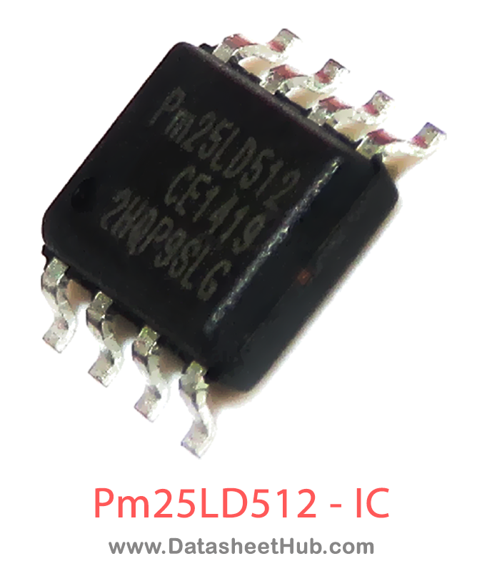
Pm25LD512 overview
The Pm25LD512 is a 512Kbit, Serial Flash Memory, supplied in an SOIC 8 pin Type package. The absolute maximum ratings table on this page lists the 7 limits from the manufacturer's datasheet that must not be exceeded. This page brings together the Pm25LD512 pinout and maximum ratings, with the full datasheet PDF to preview below or download.
The Pm25LD512/010/020 are 512Kbit/ 1Mbit / 2Mbit Serial Peripheral Interface (SPI) Flash memories, providing single- or dual-output. The devices are designed to support a 33 MHz clock rate in normal read mode, and 100 MHz in fast read, the fastest in the industry. The devices use a single low voltage power supply, wide operating voltage ranging from 2.3 Volt to 3.6 Volt, to perform read, erase and program operations. The devices can be programmed in standard EPROM programmers.
The Pm25LD512/010/020 are accessed through a 4-wire SPI Interface consisting of Serial Data Input/Output (SlO), Serial Data Output (SO), Serial Clock (SCK), and Chip Enable (CE#) pins. They comply with all recognized command codes and operations. The dual-output fast read operation provides and effective serial data rate of 200MHz.
The devices support page program mode, where 1 to 256 bytes data can be programmed into the memory in one program operation. These devices are divided into uniform 4 KByte sectors or uniform 32 KByte blocks.(Pm25LD020 is uniform 4 KByte sectors or uniform 64 KByte). The Pm25LD512/010/020 are manufactured on pFLASH™’s advanced non-volatile technology. The devices are offered in 8-pin SOIC 150mil, 8-contact WSON and 8-pin TSSOP. The devices operate at wide temperatures between -40°C to +105°C.
Datasheet
Pm25LD512 features
- Single Power Supply Operation Low voltage range: 2.3 V – 3.6 V
- Low voltage range: 2.3 V – 3.6 V
- Memory Organization
- - Pm25LD512: 64K x 8 (512 Kbit)
- - Pm25LD010: 128K x 8 (1 Mbit)
- - Pm25LD020: 256K x 8 (2 Mbit)
- Cost Effective Sector/Block Architecture
- 512Kb : Uniform 4KByte sectors / Two uniform 32KByte blocks
- 1Mb : Uniform 4KByte sectors / Four uniform 32KByte blocks
- 2Mb : Uniform 4KByte sectors / Four uniform 64KByte blocks
- Low standby current 1uA (Typ)
- Serial Peripheral Interface (SPI) Compatible
- Supports single- or dual-output
- Supports SPI Modes 0 and 3
- Maximum 33 MHz clock rate for normal read
- Maximum 100 MHz clock rate for fast read
- Page Program (up to 256 Bytes) Operation
- Typical 2 ms per page program
- Sector, Block or Chip Erase Operation
- Maximum 10 ms sector, block or chip erase
- Low Power Consumption
- Typical 10 mA active read current
- Typical 15 mA program/erase current
- Hardware Write Protection Protect and unprotect the device from write operation by Write Protect (WP#) Pin
- Protect and unprotect the device from write operation by Write Protect (WP#) Pin
- Software Write Protection The Block Protect (BP2, BP1, BP0) bits allow partial or entire memory to be configured as read- only
- The Block Protect (BP2, BP1, BP0) bits allow partial or entire memory to be configured as read- only
- High Product Endurance
- Guaranteed 200,000 program/erase cycles per single sector
- Minimum 20 years data retention
- Industrial Standard Pin-out and Package
- 8-pin 150mil SOIC
- 8-pin 208mil SOIC for Pm25LD040
- 8-pin 300mil PDIP for Pm25LD040
- 8-contact WSON
- 8-pin TSSOP
- Lead-free (Pb-free), halogen-free package
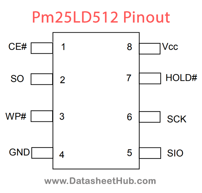
Pm25LD512 pinout
| Name | Description |
|---|---|
| CE# | Chip Enable: CE# low activates the devices internal circuitries for device operation. CE# high deselects the devices and switches into standby mode to reduce the power consumption. When a device is not selected, data will not be accepted via the serial input pin (SlO), and the serial output pin (SO) |
| SCK | Serial Data Clock |
| SIO | Serial Data Input/Output |
| SO | Serial Data Output |
| GND | Ground |
| Vcc | Device Power Supply |
| WP# | Write Protect: A hardware program/erase protection for all or part of a memory array. When the WP# pin is low, memory array write-protection depends on the setting of BP2, BP1 and BP0 bits in the Status Register. When the WP# is high, the devices are not write-protected. |
| HOLD# | Hold: Pause serial communication by the master device without resetting the serial sequence. |
Absolute maximum ratings
| Parameter | Value |
|---|---|
| Temperature Under Bias | -65oC to +125oC |
| Storage Temperature | -65oC to +125oC |
| Surface Mount Lead Soldering Temperature | Standard Package / 240oC 3 Seconds |
| Lead-free Package | 260oC 3 Seconds |
| Input Voltage with Respect to Ground on All Pins (2) | -0.5 V to VCC + 0.5 V |
| All Output Voltage with Respect to Ground | -0.5 V to VCC + 0.5 V |
| VCC (2) | -0.5 V to +6.0 V |
Pm25LD512 applications
- Data Storage
- Flash Memory
- Microcontroller Program Storage
- Firmware Updates
- Industrial Control Systems
Comments 0
Leave a comment