

RT9108NB Datasheet – 15W Stereo Audio Power Amplifier
15W Stereo Class-D Audio Power Amplifier
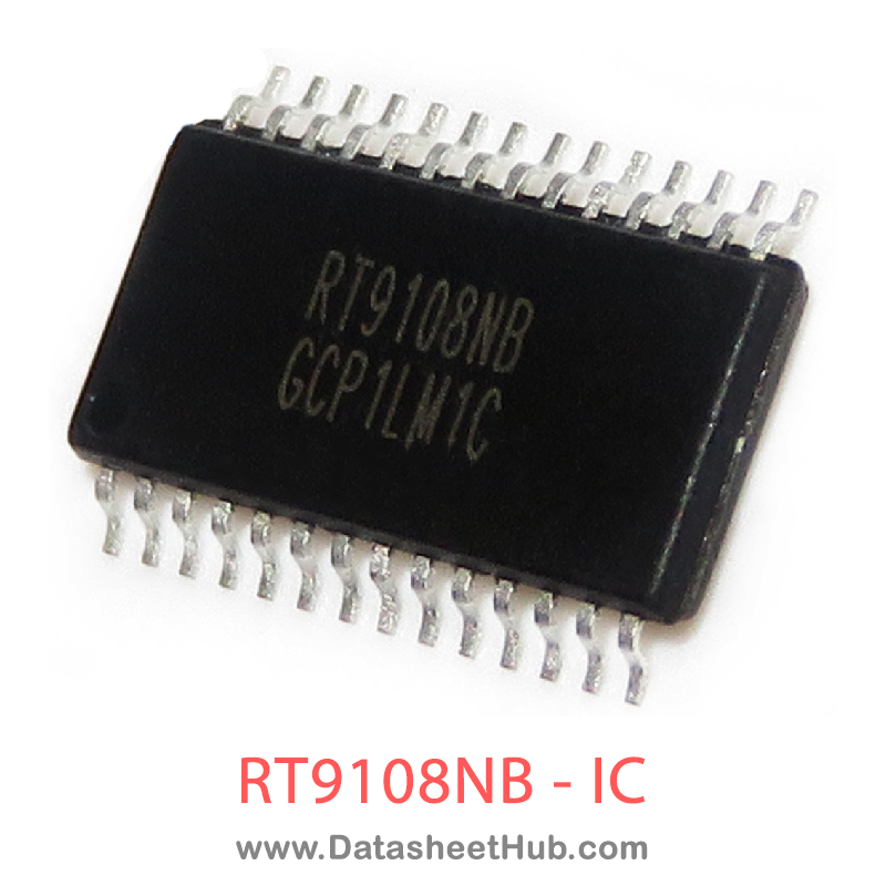
RT9108NB overview
The RT9108NB is a 15W Stereo Class-D Audio Power Amplifier made by RichTek Technology, supplied in a TSSOP-28 Pin Type package. The absolute maximum ratings table on this page lists the 11 limits from the manufacturer's datasheet that must not be exceeded. This page brings together the RT9108NB pinout and maximum ratings, with the full datasheet PDF to preview below or download.
The RT9108NB is a 15W per channel, high efficiency Class D stereo audio amplifier for driving Bridge Tied Load (BTL) speakers. The RT9108NB can drive stereo speakers with load as low as 4W. Its high efficiency eliminates the need for an extra heat sink when playing music. The gain of the amplifier can be controlled by two gain select pins. The outputs are fully protected against shorts to GND, PVCC, and output to output with an auto recovery feature and monitored output. The RT9108NB is available in a TSSOP-28 (Exposed Pad) package
Datasheet
RT9108NB features
- 8V to 26V Input Supply Range
- 6W/CH for an 8W Load, 10V Supply at 10% THD +N
- 15W/CH for an 8W Load, 16V Supply at 10% THD +N
- 90% Efficiency Eliminates Need for Heat Sinks
- Four Selectable or Fixed Gain Settings
- Mute Function Amplifier
- Robust Pin - to- Pin Short Circuit Protection
- Thermal Protection with Auto Recovery Option
- Speaker Protection with Adjustable Power Limit
- Surface Mount TSSOP-28 (Exposed Pad) Package
- RoHS Compliant and Halogen Free
RT9108NB pinout
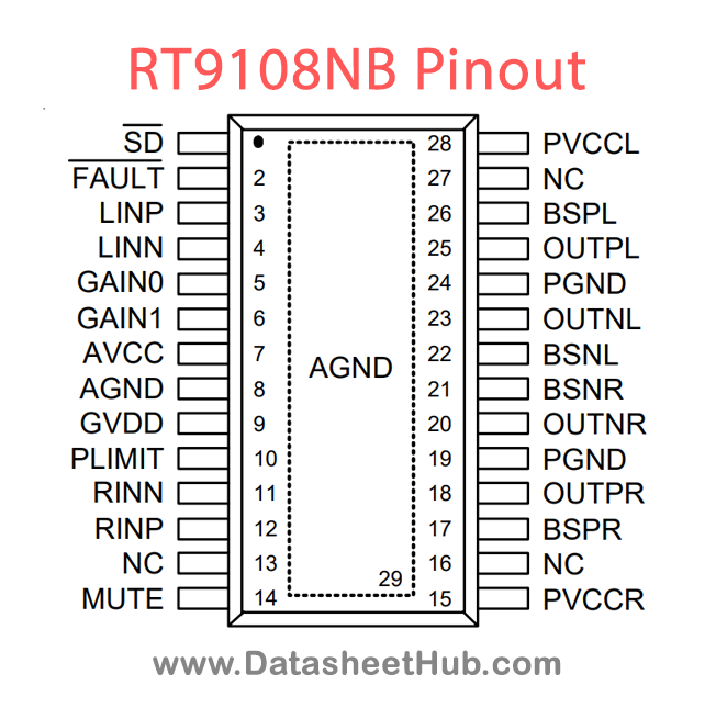
| Pin | Name | Description |
|---|---|---|
| 1 | SD | Shutdown Logic Input for Audio Amp (High = outputs enabled). TTL logic levels with compliance to AVCC. |
| 2 | FAULT | Open Drain Output for Short Circuit Fault Status. Short circuit faults can be set to auto recovery by connecting FAULT pin to SD pin. |
| 3 | LINP | Positive Audio Input for Left Channel. Biased at 2.3V. |
| 4 | LINN | Negative Audio Input for Left Channel. Biased at 2.3V. |
| 5 | GAIN0 | Gain Select Least Significant Bit. |
| 6 | GAIN1 | Gain Select Most Significant Bit. |
| 7 | AVCC | Analog Supply Input. |
| 8,29 (Exposed Pad) | AGND | Analog Ground. Connect to the thermal pad. The exposed pad must be soldered to a large PCB and connected to AGND for maximum power dissipation. |
| 9 | GVDD | High Side FET Gate Drive Supply. Nominal voltage is 5V. |
| 10 | PLIMIT | Power Limit Level Adjustment. |
| 11 | RINN | Negative Audio Input for Right Channel. Biased at 2.3V. |
| 12 | RINP | Positive Audio Input for Right Channel. Biased at 2.3V. |
| 13,16,27 | NC | No Internal Connection. |
| 14 | MUTE | Mute Logic Input for Audio Amp (Low = outputs enabled). |
| 15 | PVCCR | Power Supply Input for Right Channel H-Bridge. Right channel and left channel power supply inputs are connected internally. |
| 17 | BSPR | Bootstrap I/O for Right Channel, Positive High Side FET. |
| 18 | OUTPR | Class-D H-Bridge Positive Output for Right Channel. |
Absolute maximum ratings
| Parameter | Value |
|---|---|
| Supply Voltage, PVCCR, PVCCL, AVCC | -0.3V to 30V |
| Input Voltage, SD, GAIN0, GAIN1, FAULT | -0.3V to (AVCC + 0.3V) |
| Output Voltage, OUTPR, OUTPL, OUTNR, OUTNL | -0.3V to (PVCCx + 0.3V) |
| Bootstrap Voltage, BSPR, BSPL, BSNR, BSNL | -0.3V to (PVCCx + GVDD) |
| Other Pins | -0.3V to (GVDD + 0.3V) |
| Power Dissipation, PD @ TA = 25°CTSSOP-28 (Exposed pad) | 3.44W |
| Package Thermal ResistanceTSSOP-28 (Exposed pad), qJATSSOP-28 (Exposed pad), qJC | 29°C/W1.2°C/W |
| Junction Temperature | 150°C |
| Lead Temperature (Soldering, 10 sec.) | 260°C |
| Storage Temperature Range | -65°C to 150°C |
| ESD SusceptibilityHBM (Human Body Model) MM (Machine Model) | 2kV200V |
RT9108NB applications
- LCD-TV
- Monitors
- DVD Players
Comments 0
Leave a comment