

RT9921 Datasheet – Multi-Channel DC-DC Converter – Richtek
Integrated Multi-Channel DC-DC Converter
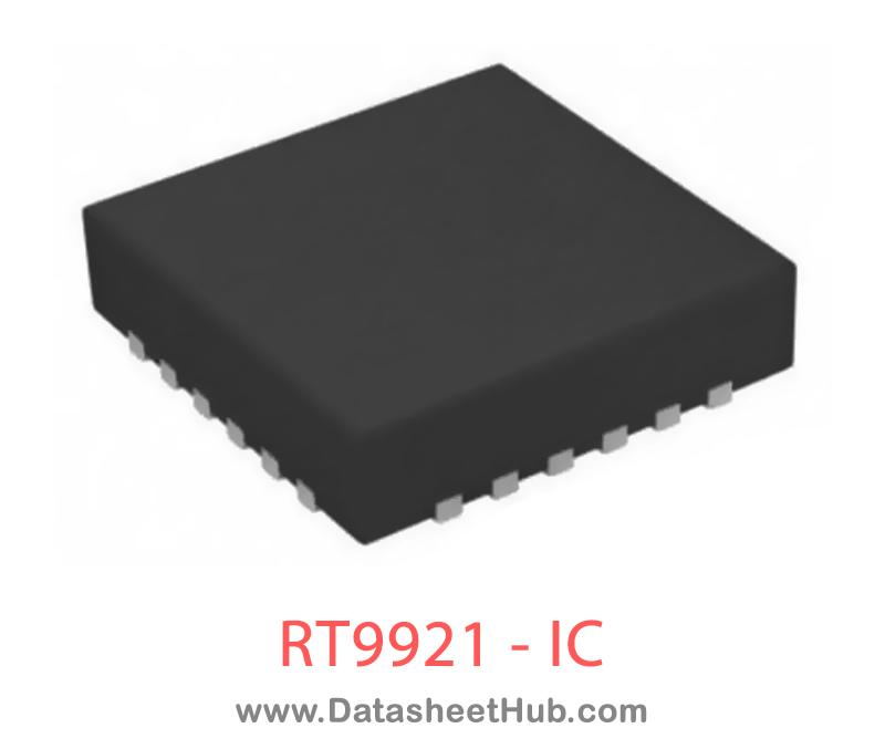
RT9921 overview
The RT9921 is an Integrated Multi-Channel DC-DC Converter made by RichTek Technology, supplied in a VQFN-24L 4×4 Type package. The absolute maximum ratings table on this page lists the 13 limits from the manufacturer's datasheet that must not be exceeded. This page brings together the RT9921 pinout and maximum ratings, with the full datasheet PDF to preview below or download.
The RT9921 includes a high-performance boost regulator, a low dropout linear regulator (LDO), a gate pulse modulator (GPM), a voltage detector, a VCOM buffer (unity- gain OPA), and a VGH charge pump controller for active- matrix thin-film transistor (TFT) liquid-crystal displays (LCDs).
The boost converter provides the regulated supply voltage for the panel source driver ICs. The converter is a high switching frequency (640kHz or 1.2MHz) current-mode regulator with an integrated 16V N-Channel 0.2L MOSFET that allows the use of ultra-small inductors and ceramic capacitors. It provides fast transient response to pulsed loading while achieving efficiency over 90%. The device can produce output voltage as high as 15V from an input as low as 2.5V. Soft-Start is programmed by external capacitor, which sets the input-current ramp-rate.
The low-dropout (LDO) linear regulator can supply up to 350mA current while input voltage is 3.3V. It uses an internal P-MOSFET as the pass device. It is suitable for the supply voltage of the timing controller.
The GPM is controlled by frame signals from timing controller to modulate the Gate-On voltage, VGHM, which acts a flicker compensation circuit to reduce the coupling effect between gate lines and pixels. It also can delay the Gate-On voltage while power-on for achieving a corrected power-on sequence for gate driver ICs. Both of power-on delay time and the falling time of the Gate-On voltage are programmable by external capacitor and resistor.
The voltage detector monitors the supply voltage to issue a reset signal while the detected voltage is too low. The detecting level is decided by an external resistor divider and the delay time is programmable by an external capacitor.
The VCOM buffer can drive the LCD VCOM voltage that features high short-circuit current (140mA), fast slew rate (12V/ms), wide bandwidth (12MHz) and rail-to-rail inputs and outputs.The VGH charge pump controller provides regulated TFT Gate-On voltage. The regulation of the positive charge pump is generated by the internal comparator that senses the output voltage and compares it with an internal reference
Datasheet
RT9921 features
- l 2.5V to 5.5V Input Supply Voltage
- 640kHz/1.2MHz Current-Mode Boost Regulator Fast Transient Response to Pulsed Load
- Fast Transient Response to Pulsed Load
- Adjustable Output Voltage (±1%) Built-In 16V, 2A, 0.2L N-MOSFET
- Built-In 16V, 2A, 0.2L N-MOSFET
- High Efficiency Up to 90% Programmable Soft-Start
- Programmable Soft-Start
- Over-Current Protection Output Under-Voltage Protection
- Output Under-Voltage Protection
- Low Dropout Voltage Linear Regulator Adjustable Output Voltage : 1.5V to VIN - 0.5V ( ±1.5%)
- Adjustable Output Voltage : 1.5V to VIN - 0.5V ( ±1.5%)
- Maximum Output Current : 350mA
- l On-Chip GPM Controller with Adjustable
- Falling Time and Power-On Delay Flicker Compensator
- Flicker Compensator
- Power-On Sequence Control
- l Low Voltage Detector
- Programmable Detecting Voltage (±2%) and Delay Time
- l Unity-Gain Operation Amplifier for VCOM Buffer
- Charge Pump for VGH regulation
- l Over-Temperature Protection
- Thin 24 Lead VQFN Package
- RoHS Compliant and 100% Lead (Pb)-Free
RT9921 pinout
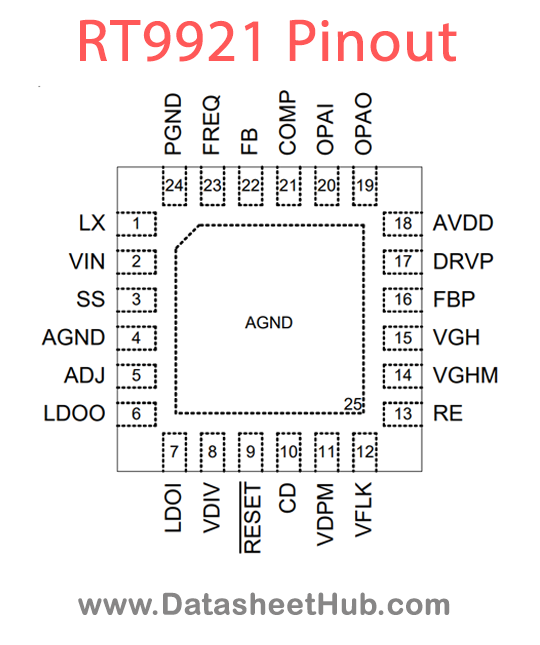
| Pin | Name | Description |
|---|---|---|
| 1 | LX | Switching Pin. Drain of the internal power N-MOSFET for the main step-up regulator. |
| 2 | VIN | Supply Input. The supply voltage powers all the control circuits including the boost converter, negative linear-regulator and gate pulse regulator and voltage detector. |
| 3 | SS | Soft-Start Control Pin. Connect a soft-start capacitor (CSS) to this pin. The soft-start capacitor is charged with a constant current 4mA. |
| 4, 25 (Exposed Pad) | AGND | Analog Ground. The exposed pad must be soldered to a large PCB and connected to GND for maximum power dissipation. |
| 5 | ADJ | Low Dropout Linear Regulator (LDO) Feedback Input. ADJ regulates to 1.24V nominal. Connect ADJ to the center of a resistive voltage divider between the LDO output voltage LDOO and the analog ground (AGND) the LDO output voltage. Place the resistive voltage divider close to the pin. |
| 6 | LDOO | Voltage Output of the LDO. |
| 7 | LDOI | Voltage Input for the LDO. |
| 8 | VDIV | Voltage Detector Divider Input. Connect VDIV to the center of a resistive voltage-divider between the detected voltage input (VDI) and analog ground (AGND). |
| 9 | RESET | Voltage Detector Output for Reset. Active Low. |
| 10 | CD | Pin for external capacitor setting the delay time for voltage detector reset delay time. The delay time tD = 120k x CD sec, where CD is the capacitance value. |
| 11 | VDPM | High-Voltage Switch Delay Input. Connect a capacitor from VDPM to GND to set the delay time. A 20mA current source charges CDPM. Power on delay time = 62k x CDPM. |
| 12 | VFLK | VFLK is produced by timing controller for charging or discharging VGHM. |
| 13 | RE | Switch Input for Discharge VGHM. |
| 14 | VGHM | VGHM is the Supply Voltage for the Gate Driver ICs. |
| 15 | VGH | Switch Input for Charge VGHM. |
| 16 | FBP | Voltage Feedback to Determine Gate-High Regulator’s Output Voltage. Connect FBP to the center of a resistive voltage-divider between the output voltage VGH and GND. Place the resistive voltage-divider close to the pin. |
| 17 | DRVP | Voltage Driver Output of Gate-High Regulator. |
| 18 | AVDD | VDD for Source Driver Power. This also supplies the GPM/OPA block. |
| 19 | OPAO | Unity-Gain OPA output pin. |
| 20 | OPAI | Unity-Gain OPA input Pin. |
| 21 | COMP | Compensation Pin for Error Amplifier. Connect a compensation network to ground. |
| 22 | FB | Main Boost Regulator Feedback Input. FB regulates to 1.24V nominal. Connect FB to the center of a resistive voltage-divider between the main output AVDD and the analog ground (AGND) the boost regulator output voltage. Place the resistive voltage divider close to the pin. |
| 23 | FREQ | Boost Converter Frequency Select Input. When FREQ is low, the oscillator frequency is set to 640kHz. When FREQ is high, the frequency is 1.2MHz. This input has a 5mA pull-down current. |
| 24 | PGND | Power Ground. PGND is the source of the power N-MOSFET. Connect PGND to the analog ground (AGND) at the device’s pins. |
Absolute maximum ratings
| Parameter | Value |
|---|---|
| Supply Input Voltage, VIN | -0.3 to 6.5V |
| LX | -0.3 to 16V |
| VGH, VGHM, RE | -0.3 to 30V |
| AVDD | -0.3 to 16V |
| VGH - AVDD, VGHM - AVDD | -0.3 to 20V |
| OPAI, OPAO, DRVP | -0.3 to (VAVDD + 0.3V) |
| VDPM, VFLK, CD, RESET, VDIV, SS, COMP, FB, FBP | -0.3 to (VIN + 0.3V) |
| LDOI | -0.3 to 6.5V |
| ADJ, LDOO | -0.3 to (LDOI+0.3V) |
| l Power Dissipation, PD @ TA = 25°CVQFN-24L 4x4 | 1.786W |
| l Package Thermal Resistance (Note 2) VQFN-24L 4x4, qJA | 56°C/W |
| Lead Temperature (Soldering, 10 sec.) | 260°C |
| l ESD Susceptibility (Note 3) HBM (Human Body Mode) 2kV MM (Machine Mode) | 2kV200V |
RT9921 applications
- LED Lighting Drivers
- Offline Power Supplies
- AC-DC Converters
- Dimmable LED Solutions
Comments 0
Leave a comment