
RTC6715 Datasheet – CMOS 5.8GHz Band FM Receiver
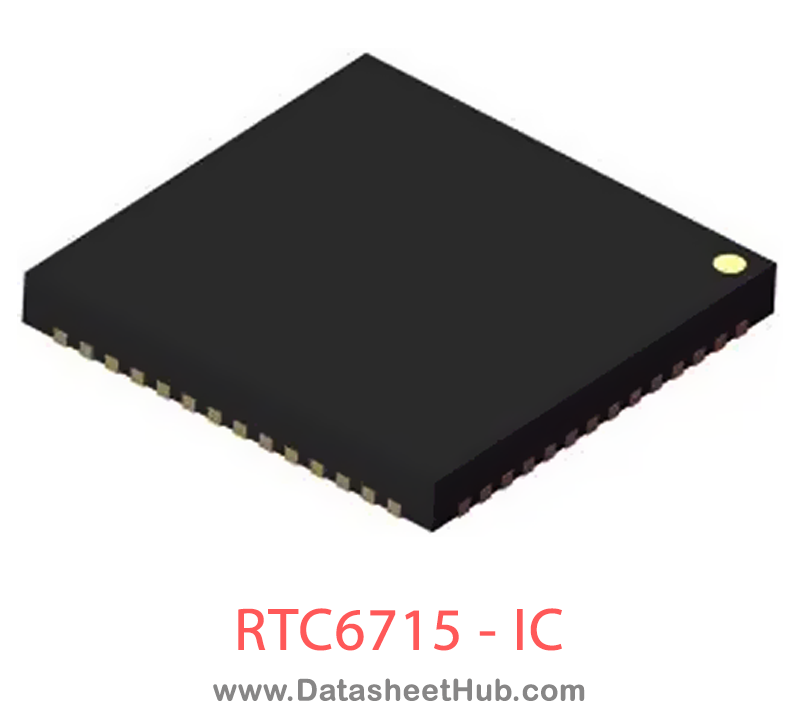
RTC6715 overview
The RTC6715 is a CMOS 5.8GHz Band FM Receiver, supplied in a 48-pin Leadless QFN package. The absolute maximum ratings table on this page lists the 5 limits from the manufacturer's datasheet that must not be exceeded. This page brings together the RTC6715 pinout and maximum ratings, with the full datasheet PDF to preview below or download.
The RTC6715 is a highly integrated FM receiver intended for application on 5.8GHz band FM demodulation. This chip includes a low noise amplifier, mixer, IF amplifier, FM demodulator, AGC, audio demodulators, audio Amps and noise squelch. With RSSI voltage output, the instantaneous radio signal strength can be monitoring. RTC6715 is able to demodulate the FM modulated video and Stereo audio signals sourced from RTC6705 and separate the desired signal at the dedicated output pins. Both Stereo and Mono application are available on the chip.
RTC6715’s operation frequency can be set by SPI programming, or by selecting six dedicated pins. Both CE and FCC regulations are easy to pass by using RTC6715 with application circuit and single room shielding case.
Datasheet
RTC6715 features
- Single 3.3V supply power
- 5.8GHz band FM demodulator with two audio subcarrier demodulators at 6MHz/6.5MHz
- High sensitivity -85dBm
- Simple six digital pins setting 24 fixed channels to eliminate external micro-controller
- Radio Strength Indicator (RSSI)
- Hard mute by noise squelch
- CMOS technology Single chip with integrated VCO and PLL
- 48-pin Leadless QFN package pass RoHS
RTC6715 pinout
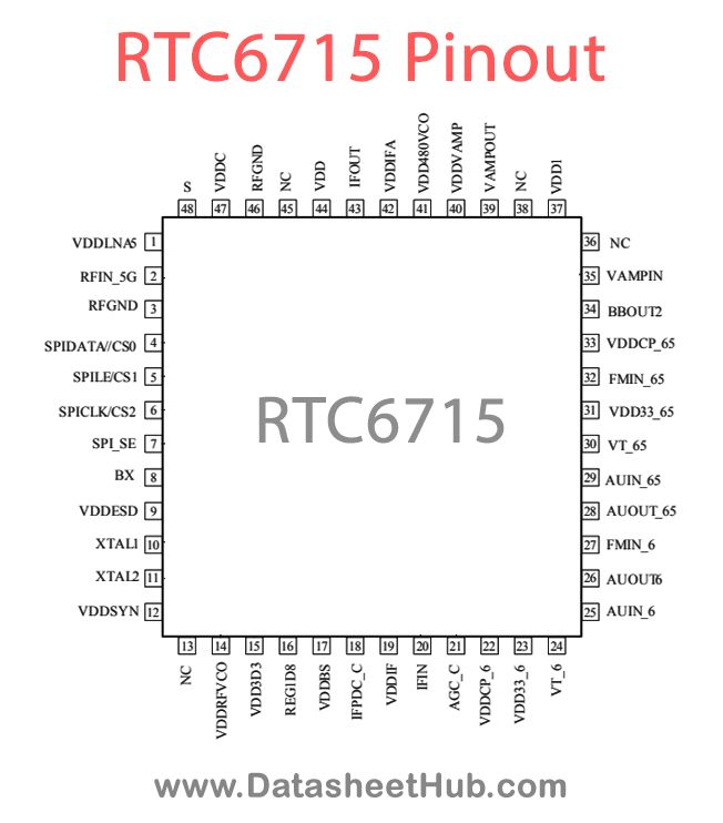
| Pin | Name | Description |
|---|---|---|
| 1 | VDDLNA5 | 3.3V for RX LNA5G |
| 2 | RFIN_5G | 5 GHz LNA input for RF input signal |
| 3 | RFGND | RF ground |
| 4 | CS0 | Easy channel selection (Internal pull high) 1 |
| SPIDATA | Digital In | |
| 5 | CS1 | Easy channel selection (Internal pull high) 1 |
| SPILE | Digital In | |
| 6 | CS2 | Easy channel selection (Internal pull high) 1 |
| SPICLK | Digital In | |
| 7 | SPI_SE | Switch mode or SPI selection 1 |
| 8 | BX | At easy channel selection mode : BX is used for alternative band selection 1 At SPI mode : BX is Don’t care |
| 9 | VDDESD | 3.3V |
| 10 | XTAL1 | Crystal Input |
| 11 | XTAL2 | Crystal Input |
| 12 | VDDSYN | 3.3V for RF synthesizer |
| 13 | NC | Not connected |
| 14 | VDDRFVCO | 3.3V for 5GHz VCO |
| 15 | VDD3D3 | 3.3V for digital 1.8V regulator |
| 16 | REG1D8 | Regulator 1.8V for Digital block |
| 17 | VDDBS | 3.3V for Bias |
| 18 | IFPDC_C | RSSI Out |
| 19 | VDDIF | 3.3V for IFAAF |
| 20 | IFIN | IFA_AF inputs |
| 21 | AGC_C | AGC Rectifier output |
Show all 51 pins
| Pin | Name | Description |
|---|---|---|
| 22 | VDDCP_6 | 3.3V for 6MHz charge pump and VCO |
| 23 | VDD33_6 | 3.3V for 6MHz audio amplifier |
| 24 | VT_6 | Audio demo out for 6MHz VCO |
| 25 | AUIN_6 | Audio amplifier in for 6MHz path |
| 26 | AUOUT6 | Audio amplifier out for 6MHz path |
| 27 | FMIN_6 | 6MHz FM audio in |
| 28 | AUOUT_65 | Audio amplifier out for 6.5MHz path |
| 29 | AUIN_65 | Audio amplifier in for 6.5MHz path |
| 30 | VT_65 | Audio demo out for 6.5MHz VCO |
| 31 | VDD33_65 | 3.3V for 6.5MHz audio amplifier |
| 32 | FMIN_65 | 6.5MHz FM audio in |
| 33 | VDDCP_65 | 3.3V for 6.5MHz charge pump and VCO |
| 34 | BBOUT2 | FMDeMod Buffer output |
| 35 | VAMPIN | Video amp input |
| 36 | NC | Not connected |
| 37 | VDD1 | 3.3V |
| 38 | NC | Not connected |
| 39 | VAMPOUT | Video amp output |
| 40 | VDDVAMP | 3.3V for Video Amp |
| 41 | VDD480VCO | 3.3V for FM demod VCO |
| 42 | VDDIFA | 3.3V for RX IFAs |
| 43 | IFOUT | IF OUT |
| 44 | VDD | 3.3V VDD |
| 45 | NC | Not connected |
| 46 | RFGND | RF ground |
| 47 | NC | Not connected |
| 48 | S | A/B band selection 1 0 for A band; 1 for B band |
Absolute maximum ratings
| Parameter | Symbol | Value | Unit |
|---|---|---|---|
| Storage Temperature Range | Tstr | -65 to +150 | °C |
| Operating Temperature Range | Totr | -40 to +85 | °C |
| Supply Voltage | Vdd | -0.5 to +5 | V |
| Logic control signal | Vlog | -0.5 to +5 | V |
| RX input | VRX | -2 to +2 | V |
RTC6715 applications
- AV Sender
- Surveillance
- Baby Monitor
- Wireless Camera
- Wireless Audio
- Wireless Earphone
Comments 0
Leave a comment