
STN1170 Datasheet – Multiprotocol OBD to UART Interpreter
OBD to UART interpreter IC

STN1170 overview
The STN1170 is an OBD to UART interpreter IC, supplied in a 44 Pin TQFP ( STN1170-I/PT ) and 44 QFN ( STN1170-I/ML ) Type package. The absolute maximum ratings table on this page lists the 6 limits from the manufacturer's datasheet that must not be exceeded. This page brings together the STN1170 pinout and maximum ratings, with the full datasheet PDF to preview below or download.
The STN1170 is an OBD to UART interpreter IC designed to provide bi-directional half-duplex commu- nication with the vehicle’s On-Board Diagnostic system (OBD-II). It supports all legislated OBD-II protocols, as well as two proprietary networks: GM Single Wire CAN (GMLAN), and Ford Medium Speed CAN (MS CAN).
A wealth of information can be obtained by tapping into the OBD bus, including the status of the malfunction indicator light (MIL), diagnostic trouble codes (DTCs), inspection and maintenance (I/M) information, freeze frames, VIN, hundreds of real-time parameters, and more.
The STN1170 is fully compatible with the de facto industry standard ELM327 command set. Based on a 16-bit processor core, the STN1170 offers more features and better performance than any other ELM327 compatible IC.
Datasheet
STN1170 features
- Stable, field-tested firmware
- Fully compatible with the ELM327 AT command set
- Fully backwards compatible with the STN1110 command set
- Extended ST command set
- UART interface (baud rates from 38 bps to 10 Mbps1)
- Secure bootloader for easy firmware updates
- Support for all legislated OBD-II protocols
- ISO 15765-4 (CAN)
- ISO 14230-4 (Keyword Protocol 2000)
- ISO 9141-2 (Asian, European, Chrysler vehicles)
- SAE J1850 VPW (GM vehicles)
- SAE J1850 PWM (Ford vehicles)
- Support for non-legislated OBD protocols:ISO 15765
- ISO 15765
- ISO 11898 (raw CAN)
- GMLAN Single Wire CAN (GMW3089)
- Ford Medium Speed CAN (MS CAN)
- Support for the heavy-duty SAE J1939 OBD protocol
- Superior automatic protocol detection algorithm
- Large message buffer
- Sophisticated Power Save Sleep/Wakeup Triggers
- Available in TQFP and QFN packages
- RoHS compliant
STN1170 pinout
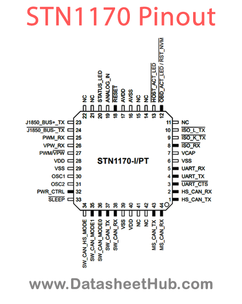
| Pin | Name | Description |
|---|---|---|
| 1 | HS_CAN_TX | High-speed CAN transmit output |
| 2 | HS_CAN_RX | High-speed CAN receive input |
| 3 | UART_CTS | Active low UART clear to send input |
| 4 | UART_TX | UART transmit output |
| 5 | UART_RX | UART receive input |
| 6 | VSS | Ground reference for logic and I/O pins |
| 7 | VCAP | CPU logic filter capacitor connection |
| 8 | ISO _RX | Active low ISO 9141/ISO 14230 K-line input |
| 9 | ISO _K_TX | Active low ISO 9141/ISO 14230 K-line output |
| 10 | ISO_L_TX | Active low ISO 9141/ISO 14230 L-line output |
| 11 | NC | Do not connect |
| 12 | OBD_ACT_LED/ RST_NVM | Active low OBD activity LED output and active low input to reset non-volatile settings to factory defaults |
| 13 | HOST_ACT_LED | Active low host activity LED output |
| 14 | NC | Do not connect |
| 15 | NC | Do not connect |
| 16 | AVSS | Analog ground reference |
| 17 | AVDD | Analog positive supply |
| 18 | RESET | Active low device reset input |
| 19 | ANALOG_IN | Analog voltage measurement input |
| 20 | STATUS_LED | Status LED output |
| 21 | NC | Do not connect |
| 22 | NC | Do not connect |
| 23 | J1850_BUS+_TX | SAE J1850 Bus+ transmit output |
| 24 | J1850_BUS-_TX | Active low SAE J1850 Bus- transmit output |
Show all 33 pins
| Pin | Name | Description |
|---|---|---|
| 25 | PWM_RX | SAE J1850 PWM receive input |
| 26 | VPW_RX | SAE J1850 VPW receive input |
| 27 | PWM/VPW | SAE J1850 PWM/VPW Bus+ voltage select output |
| 28 | VDD | Positive supply for logic and I/O pins |
| 29 | VSS | Ground reference for logic and I/O pins |
| 30 | OSC1 | 16.000 MHz oscillator crystal input |
| 31 | OSC2 | 16.000 MHz oscillator crystal output |
| 32 | PWR_CTRL | External power control output |
| 33 | SLEEP | External sleep control input |
Absolute maximum ratings
| Parameter | Value |
|---|---|
| Ambient temperature under bias | -40°C to +125°C |
| Storage temperature | -65°C to +160°C |
| Voltage on any pin that is not 5V tolerant with respect to VSS | 0.3V to (VDD + 0.3V) |
| Maximum current sourced/sunk by any 2x output (3) | 8 mA |
| Maximum current sourced/sunk by any 4x output (3) | 15 mA |
| Maximum current sourced/sunk by any 8x output (3) | 25 mA |
STN1170 applications
- Vehicle telematics
- Fleet management and tracking applications
- Usage-based insurance (UBI)
- OBD data loggers
- Automotive diagnostic scan tools and code readers
- Digital dashboards
Comments 0
Leave a comment