

TC74ACT541FT Datasheet – Octal Bus Buffer IC
Non-Inverting Octal Bus Buffer

TC74ACT541FT overview
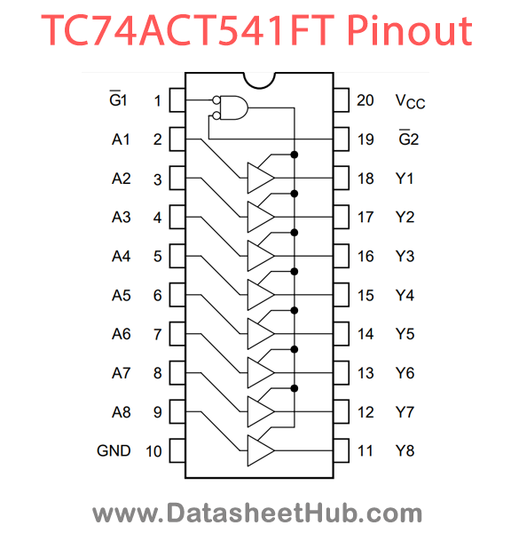
The TC74ACT541FT is a Non-Inverting Octal Bus Buffer made by Toshiba, supplied in these packages: DIP, SOP 20 Pin Type. The absolute maximum ratings table on this page lists the 9 limits from the manufacturer's datasheet that must not be exceeded. This page brings together the TC74ACT541FT pinout and maximum ratings, with the full datasheet PDF to preview below or download.
The TC74ACT540/TC74ACT541 are advanced high speed CMOS OCTAL BUS BUFFERs fabricated with silicon gate and double-layer metal wiring C2MOS technology.
They achieve the high speed operation similar to equivalent Bipolar Schottky TTL while maintaining the CMOS low power dissipation.
These devices may be used as a level converter for interfacing TTL or NMOS to High Speed CMOS. The inputs are compatible with TTL, NMOS and CMOS output voltage levels.
The TC74ACT540 is an inverting type, and the TC74ACT541 is a non-inverting type. When either G1 or G2 are high, the terminal outputs are in the high-impedance state. All inputs are equipped with protection circuits against static discharge or transient excess voltage.
Datasheet
TC74ACT541FT features
- High speed: tpd = 4.3 ns (typ.) at VCC = 5 V
- Low power dissipation: ICC = 8 mA (max) at Ta = 25°C
- Compatible with TTL outputs
- VIL = 0.8 V (max) VIH = 2.0 V (min)
- Symmetrical output impedance
- |IOH| = IOL = 24 mA (min)
- Capability of driving 50 W transmission lines.
- Balanced propagation delays: tpLH -~ tpHL
- Pin and function compatible with 74F540/541
TC74ACT541FT pinout
Absolute maximum ratings
| Parameter | Symbol | Value | Unit |
|---|---|---|---|
| Supply voltage range | VCC | -0.5 to 7.0 | V |
| DC input voltage | VIN | -0.5 to VCC + 0.5 | V |
| DC output voltage | VOUT | -0.5 to VCC + 0.5 | V |
| Input diode current | IIK | ±20 | mA |
| Output diode current | IOK | ±50 | mA |
| DC output current | IOUT | ±50 | mA |
| DC VCC/ground current | ICC | ±200 | mA |
| Power dissipation | PD | 500 (DIP) (Note 2)/180 (SOP/TSSOP) | mW |
| Storage temperature | Tstg | -65 to 150 | °C |
TC74ACT541FT applications
- Digital Logic Level Shifting
- Buffering and Line Driving
- Signal Isolation
- Data Bus Communication
Comments 0
Leave a comment