

TDA8763A Datasheet – 10-bit High Speed Low Power ADC IC
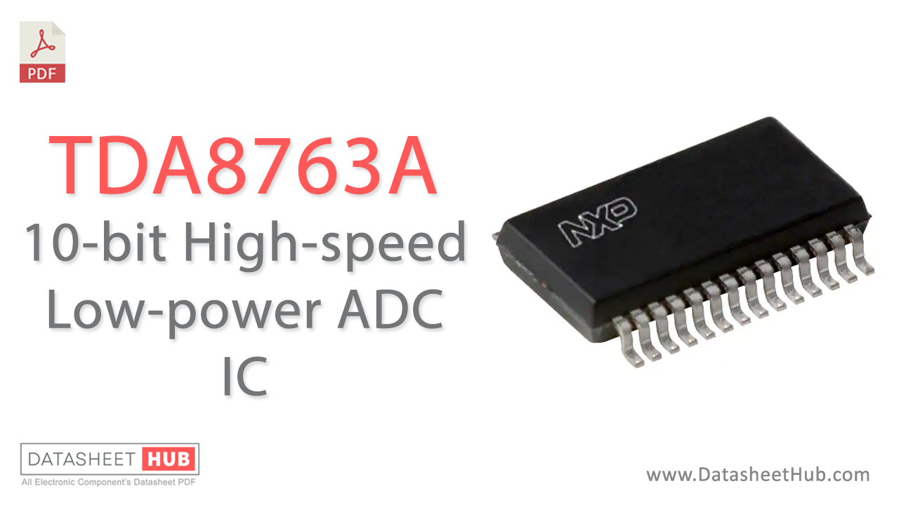
TDA8763A overview
The TDA8763A is a 10-bit high-speed low-power analog-to-digital converter (ADC) for professional video and other applications. It converts the analog input signal into 10-bit binary-coded digital words at a maximum sampling rate of 50 MHz. All digital inputs and outputs are TTL and CMOS compatible, although a low-level sine wave clock input signal is allowed.
The device requires an external source to drive its reference ladder. If the application requires that the reference is driven via internal sources the recommendation is to use the TDA8763.
| Part Number | TDA8763A |
| Function | 10-bit High-speed Low-power ADC |
| Package | SSOP 28 Pin Type |
| Manufacturer | Philips Electronics - NXP |
| Datasheet | Download PDF  |
Datasheet
TDA8763A features
- 10-bit resolution
- Sampling rate up to 50 MHz
- DC sampling allowed
- One clock cycle conversion only
- No missing codes guaranteed
- In-Range (IR) CMOS output
- Levels TTL and CMOS-compatible digital inputs
- 3 to 5 V CMOS digital outputs
- Low-level AC clock input signal allowed
- External reference voltage regulator
- Power dissipation is only 175 mW (typical)
- Low analog input capacitance, no buffer amplifier required
- No sample-and-hold circuit is required.
TDA8763A pinout
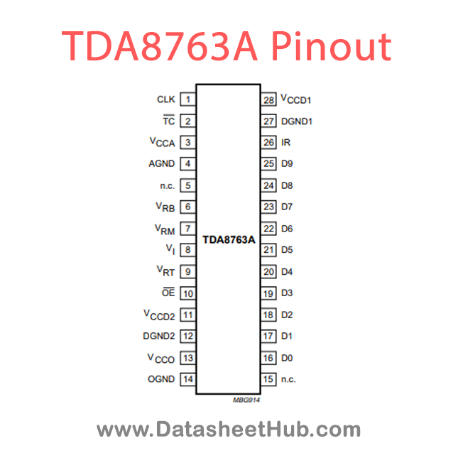
| Pin | Name | Description |
|---|---|---|
| 1 | CLK | clock input |
| 2 | TC | twos complement input (active LOW) |
| 3 | VCCA | analog supply voltage (+5 V) |
| 4 | AGND | analog ground |
| 5 | NC | not connected |
| 6 | VRB | reference voltage BOTTOM input |
| 7 | VRM | reference voltage MIDDLE input |
| 8 | VI | analog input voltage |
| 9 | VRT | reference voltage TOP input |
| 10 | OE | output enable input (CMOS levelinput, active LOW) |
| 11 | VCCD2 | digital supply voltage 2 (+5 V) |
| 12 | DGND2 | digital ground 2 |
| 13 | VCCO | supply voltage for output stages (3 to 5 V) |
| 14 | OGND | output ground |
| 15 | NC | not connected |
| 16 to 25 | D0 to D9 | data output; bit 0 To 9 |
| 26 | IR | in range data output |
| 27 | DGND1 | digital ground 1 |
| 28 | VCCD1 | digital supply voltage 1 (+5 V) |
TDA8763A applications
- Video data digitizing
- Radar pulse analysis
- Transient signal analysis
- High-energy physics research
- Σ∆ modulators
- Medical imaging.
More about TDA8763A
TDA8763A Limiting Values
In accordance with the Absolute Maximum Rating System (IEC 134).
| SYMBOL | PARAMETER | CONDITIONS | MIN. | MAX. | UNIT |
| VCCA | analog supply voltage | note 1 | -0.3 | +7.0 | V |
| VCCD | digital supply voltage | note 1 | -0.3 | +7.0 | V |
| VCCO | output stages supply voltage | note 1 | -0.3 | +7.0 | V |
| DVCC | supply voltage difference VCCA - VCCD VCCA - VCCO VCCD - VCCO | -1.0 -1.0 -1.0 | +1.0 +4.0 +4.0 | V V V | |
| VI | input voltage | referenced to AGND | -0.3 | +7.0 | V |
| Vi(sw)(p-p) | AC input voltage for switching (peak-to-peak value) | referenced to DGND | - | VCCD | V |
| IO | output current | - | 10 | mA | |
| Tstg | storage temperature | -55 | +150 | °C | |
| Tamb | operating ambient temperature | -40 | +85 | °C | |
| Tj | junction temperature | - | 150 | °C |
Note
1. The supply voltages VCCA, VCCD, and VCCO may have any value between -0.3 V and +7.0 V provided that the supply voltage differences DVCC are respected.
Comments 0
Leave a comment