

TDA8768A Datasheet PDF – 12-bit, Analog-to-Digital Converter
12-bit, 70 Msps high-speed Analog-to-Digital Converter (ADC)
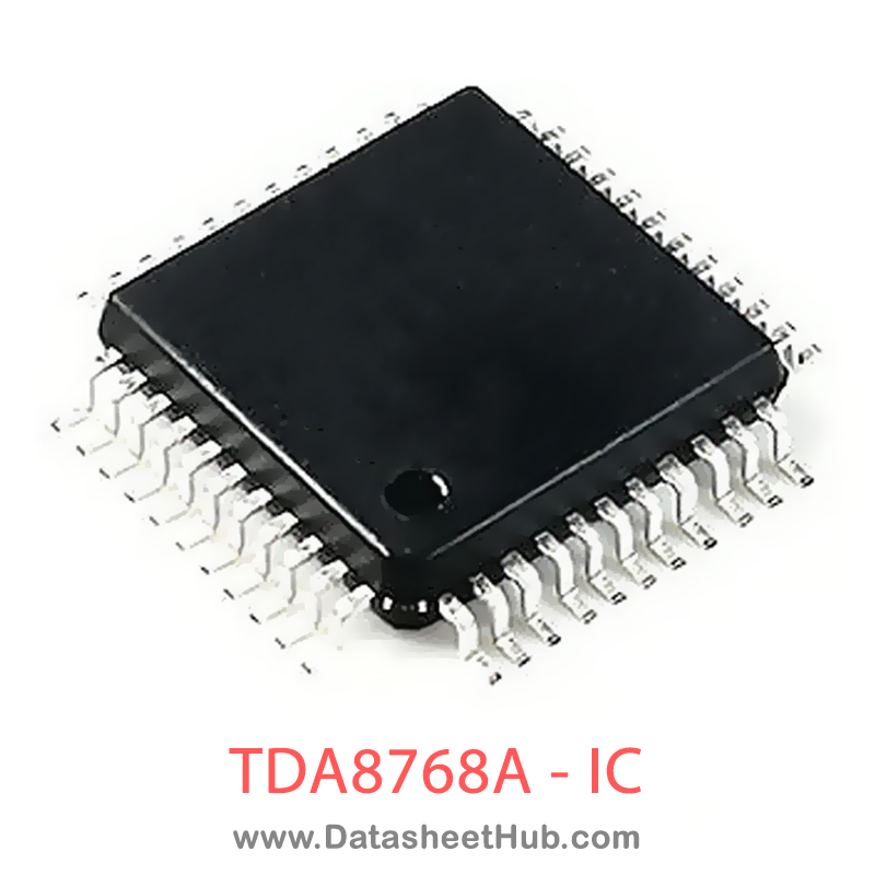
TDA8768A overview
The TDA8768A is a 12-bit, 70 Msps high-speed Analog-to-Digital Converter (ADC) made by Philips Electronics - NXP, supplied in a QFP44 Type package. The absolute maximum ratings table on this page lists the 12 limits from the manufacturer's datasheet that must not be exceeded. This page brings together the TDA8768A pinout and maximum ratings, with the full datasheet PDF to preview below or download.
The TDA8768AH is a biCMOS 12-bit Analog-to-Digital Converter (ADC) optimized for GSM and EDGE cellular infrastructures, professional telecommunications and imaging, and advanced FM radio. It converts the analog input signal into 12-bit binary coded digital words at a maximum sampling rate of 70 MHz. All static digital inputs (SH, CE and OTC) are TTL and CMOS compatible and all outputs are CMOS compatible. A sine wave clock input signal can also be used.
Datasheet
TDA8768A features
- 12-bit resolution
- Sampling rate up to 70 MHz
- -3 dB bandwidth of 245 MHz
- 5 V power supplies and 3.3 V output power supply
- Binary or twos complement CMOS outputs
- In-range CMOS compatible output
- TTL and CMOS compatible static digital inputs
- TTL and CMOS compatible digital outputs
- Differential AC or PECL clock input; TTL compatible
- Power dissipation 550 mW (typical)
- Low analog input capacitance (typical 2 pF), no buffer amplifier required
- Integrated sample-and-hold amplifier
- Differential analog input
- External amplitude range control
- Voltage controlled regulator included
- -40 °C to +85 °C ambient temperature.
TDA8768A pinout
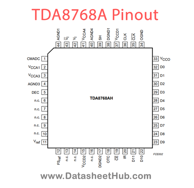
| Pin | Name | Description |
|---|---|---|
| 1 | CMADC | regulator output common mode ADC input |
| 2 | VCCA1 | analog supply voltage 1 (+5 V) |
| 3 | VCCA3 | analog supply voltage 3 (+5 V) |
| 4 | AGND3 | analog ground 3 |
| 5 | DEC | decoupling node |
| 6 | NC | not connected |
| 7 | NC | not connected |
| 8 | NC | not connected |
| 9 | NC | not connected |
| 10 | NC | not connected |
| 11 | VREF | reference voltage input |
| 12 | FSREF | full-scale reference output |
Absolute maximum ratings
| Parameter | Symbol | Value | Unit | Conditions |
|---|---|---|---|---|
| Analog supply voltage | VCCA | Min -0.3 / Max +7.0 | V | |
| Digital supply voltage | VCCD | Min -0.3 / Max +7.0 | V | |
| Output supply voltage | VCCO | Min -0.3 / Max +7.0 | V | |
| VCCA - VCCD | Min -1.0 / Max +1.0 | V | ||
| VCCD - VCCO | Min -1.0 / Max +4.0 | V | ||
| VCCA - VCCO | Min -1.0 / Max +4.0 | V | ||
| input voltage at pins 42 and 43 | VI, VI | Min 0.3 / Max VCCA | V | referenced to AGND |
| input voltage at pins 35 and 36 for differential | VCLK(p-p) | Max VCCD | V | |
| output current | IO | Max 10 | mA | |
| storage temperature | Tstg | Min -55 / Max +150 | °C | |
| ambient temperature | Tamb | Min -40 / Max +85 | °C | |
| junction temperature | Tj | Max 150 | °C |
TDA8768A applications
- High-speed analog-to-digital conversion for
- Cellular infrastructure (GSM and EDGE)
- Professional telecommunication
- Advanced FM radio
- Radar
- Imaging (camera scanner)
- Set Top Box (STB)
- Medical imaging.
Comments 0
Leave a comment