

TDA8786A Datasheet – 10-Bit Analog-to-Digital IC
10-Bit Analog-to-Digital Interface for CCD cameras.
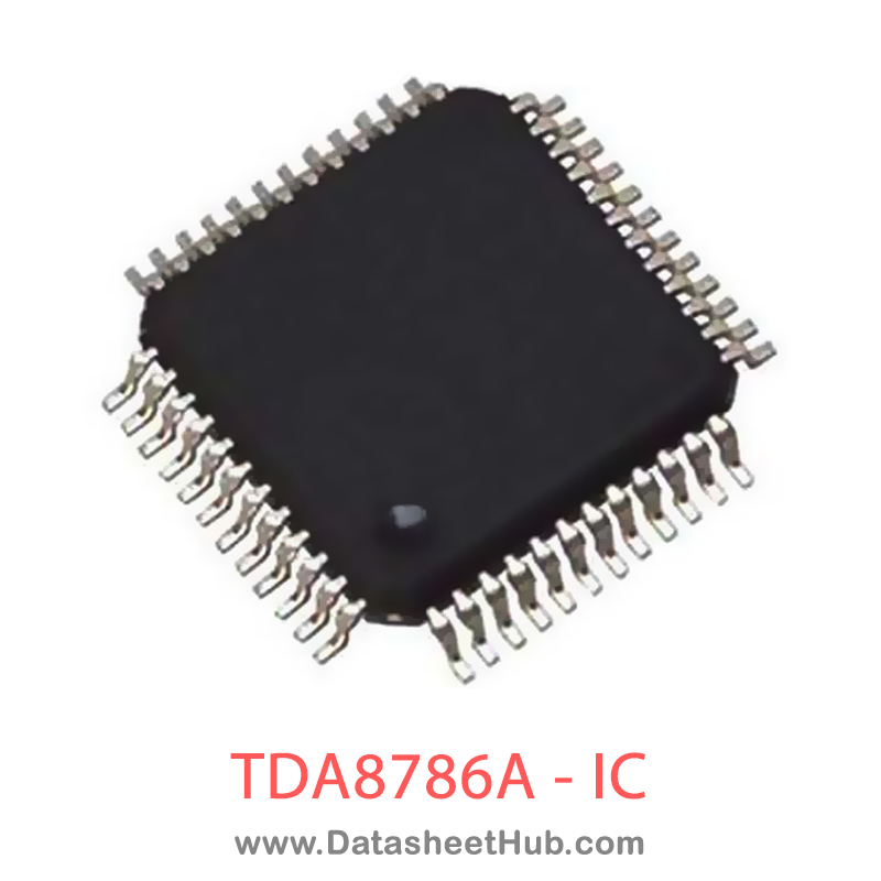
TDA8786A overview
The TDA8786A is a 10-Bit Analog-to-Digital Interface for CCD cameras. made by Philips Electronics - NXP, supplied in an LQFP 48 Pin Type package. Main ratings: analog supply voltage Min. -0.3 / Max. +7.0; digital supply voltage Min. -0.3 / Max. +7.0; output stages supply voltage Min. -0.3 / Max. +7.0; supply voltage difference between VCCA and VCCD between VCCA and VCCO between VCCD and VCCO Min. -1.0 -1.0 -1.0 / Max. +1.0 +4.0 +4.0. This page brings together the TDA8786A pinout and key specifications, with the full datasheet PDF to preview below or download.
The TDA8786; TDA8786A is a 10-bit analog-to-digital interface for CCD cameras. The device includes a correlated double sampling circuit, AGC, a soft clipper circuit and a low power 10-bit Analog-to-Digital Converter (ADC) together with its reference voltage regulator.
The AGC and soft clipper circuits are controlled by on-chip DACs via a serial interface.
A 10-bit DAC controls the ADC input clamp level.
An additional DAC is provided for additional system controls; its output voltage range is 1.4 V (p-p) which is available at pin OFDOUT
Key specifications
Datasheet
TDA8786A features
- Correlated Double Sampling (CDS), AGC, soft clipper, pre-blanking, 10-bit ADC and reference regulator included
- Fully programmable via a 3-wire serial interface
- Sampling frequency up to 18 MHz
- AGC gain from 3.5 to 33.5 dB (in 0.1 dB steps)
- Programmable soft clipper for white compression (starting at 40% of the input signal)
- Standby mode available for each block for power saving applications (19 mW)
- 6 dB fixed gain analog output for analog iris control
- 8-bit and 10-bit DAC included for analog settings
- Low power consumption of only 475 mW (typ.)
- 5 V operation and 2.5 to 5 V operation for the digital outputs
- CDS control pulse: TDA8786 = HIGH; TDA8786A = LOW
- TTL compatible inputs, TTL and CMOS compatible outputs
TDA8786A pinout
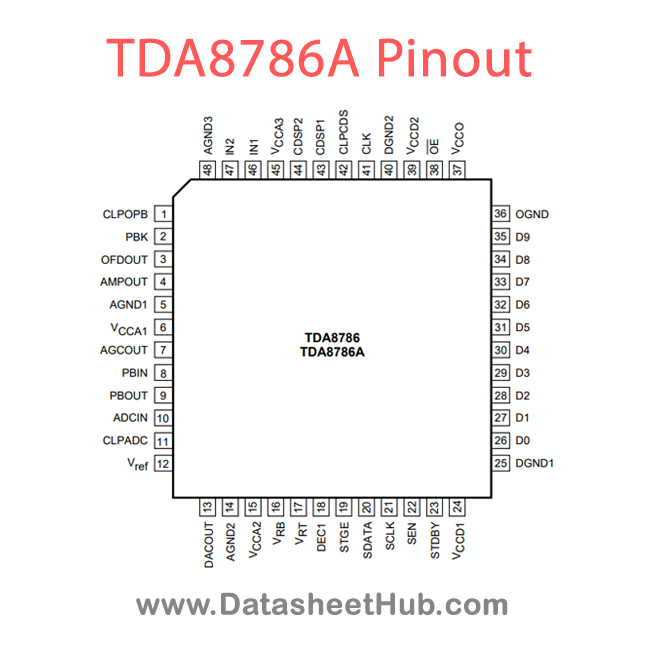
| Pin | Name | Description |
|---|---|---|
| 1 | CLPOPB | optical black clamp control pulse input (active HIGH for TDA8786, active LOW for TDA8786A) |
| 2 | PBK | pre-blanking control pulse input; if PBK is HIGH (LOW) the signal is replaced by the optical black level for TDA8786 (TDA8786A) |
| 3 | OFDOUT | analog output of the additional 8-bit control DAC (controlled via the serial interface) |
| 4 | AMPOUT | CDS amplifier output (fixed gain = +6 dB) |
| 5 | AGND1 | analog ground 1 |
| 6 | VCCA1 | analog supply voltage 1 |
| 7 | AGCOUT | AGC and soft clipper amplifier signal output |
| 8 | PBIN | optical black clamp and pre-blanking block signal input (from AGCOUT via a capacitor) |
| 9 | PBOUT | optical black clamp and pre-blanking block signal output |
| 10 | ADCIN | ADC analog signal input (from PBOUT or AGCOUT via a capacitor) |
| 11 | CLPADC | clamp control input for ADC analog input signal clamp (active HIGH for TDA8786 and active LOW for TDA8786A) |
| 12 | Vref | ADC input clamp reference voltage (normally connected to pin VRB or DACOUT) |
| 13 | DACOUT | DAC output for ADC clamp level |
| 14 | AGND2 | analog ground 2 |
| 15 | VCCA2 | analog supply voltage 2 |
| 16 | VRB | ADC reference voltage (BOTTOM) code 0 |
| 17 | VRT | ADC reference voltage (TOP) code 1023 |
| 18 | DEC1 | decoupling 1 (decoupled to ground via a capacitor) |
| 19 | STGE | CDS offset storage |
| 20 | SDATA | serial data input for the 4 control DACs (9-bit DAC for AGC gain, 4-bit DAC for soft clipper; additional 8-bit DAC for OFD output voltage; 10-bit DAC for ADC clamp level and the stand-by mode per block; see Table 1) |
| 21 | SCLK | serial clock input for the control DACs and their serial interface; see Table 1 |
| 22 | SEN | enable input for the serial interface shift register (active when SEN = logic 0); see Table 1 |
| 23 | STDBY | stand-by control pin (active HIGH); all the output bits are logic 0 when stand-by is enabled |
| 24 | VCCD1 | digital supply voltage 1 |
Show all 36 pins
| Pin | Name | Description |
|---|---|---|
| 25 | DGND1 | digital ground 1 |
| 26 | D0 | ADC digital output 0 (LSB) |
| 27 | D1 | ADC digital output 1 |
| 28 | D2 | ADC digital output 2 |
| 29 | D3 | ADC digital output 3 |
| 30 | D4 | ADC digital output 4 |
| 31 | D5 | ADC digital output 5 |
| 32 | D6 | ADC digital output 6 |
| 33 | D7 | ADC digital output 7 |
| 34 | D8 | ADC digital output 8 |
| 35 | D9 | ADC digital output 9 (MSB) |
| 36 | OGND | digital output ground |
TDA8786A specifications
| analog supply voltage | Min. -0.3 / Max. +7.0 V note 1 |
|---|---|
| digital supply voltage | Min. -0.3 / Max. +7.0 V note 1 |
| output stages supply voltage | Min. -0.3 / Max. +7.0 V note 1 |
| supply voltage difference between VCCA and VCCD between VCCA and VCCO between VCCD and VCCO | Min. -1.0 -1.0 -1.0 / Max. +1.0 +4.0 +4.0 V V V |
| input voltage | Min. -0.3 / Max. +7.0 V referenced to VSSA |
| AC input voltage for switching (peak-to peak-value) | Max. VCCD V referenced to VSSD |
| output current | Max. 10 mA |
| storage temperature | Min. -55 / Max. +150 °C |
| operating ambient temperature | Min. -20 / Max. +75 °C |
| junction temperature | Max. 150 °C |
TDA8786A applications
- CCD camera systems.
- Digital Audio Processors
- Audio Signal Conversion
- Sound Processing Systems
- Digital-to-Analog Converter (DAC)
Comments 0
Leave a comment