

TL555I Datasheet – LinCMOS Timer IC

TL555I overview
The TLC555 is a monolithic timing circuit fabricated using the TI LinCMOS™ process. The timer is fully compatible with CMOS, TTL, and MOS logic and operates at frequencies up to 2 MHz. Because of its high input impedance, this device supports smaller timing capacitors than those supported by the NE555 or LM555. As a result, more accurate time delays and oscillations are possible.
Power consumption is low across the full range of power-supply voltage.
Like the NE555, the TLC555 has a trigger level equal to approximately one-third of the supply voltage and a threshold level equal to approximately two-thirds of the supply voltage. These levels can be altered by the use of the control voltage terminal (CONT). When the trigger input (TRIG) falls below the trigger level, the flip-flop is set and the output goes high. If TRIG is above the trigger level and the threshold input (THRES) is above the threshold level, the flip-flop is reset and the output is low. The reset input (RESET) can override all other inputs and can be used to initiate a new timing cycle. If RESET is low, the flip-flop is reset and the output is low. Whenever the output is low, a low-impedance path is provided between the discharge terminal (DISCH) and GND. All unused inputs must be tied to an appropriate logic level to prevent false triggering
| Part Number | TL555I, TL555IID, TL555IDR ( Marking TL555I ) |
| Function | LinCMOS Timer |
| Package | SOIC 8 Pin |
| Manufacturer | Texas Instruments |
| Datasheet | Download PDF  |
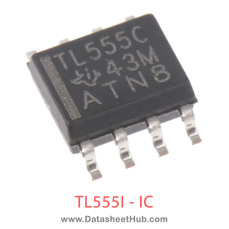
Datasheet
TL555I features
- Very low power consumption: 1-mW typical at VDD = 5 V
- 1-mW typical at VDD = 5 V
- Capable of operation in astable mode
- CMOS output capable of swinging rail to rail
- High output current capability Sink: 100-mA typical Source: 10-mA typical
- Sink: 100-mA typical
- Source: 10-mA typical
- Output fully compatible with CMOS, TTL, and MOS
- Low supply current reduces spikes during output transitions
- Single-supply operation from 2 V to 15 V
- Functionally interchangeable with the NE555; has the same pinout
- ESD protection exceeds 2000 V per MIL-STD- 883C, method 3015.2
- Available in Q-temp automotive
- High-reliability automotive applications
- Configuration control and print support
- Qualification to automotive standards
TL555I pinout
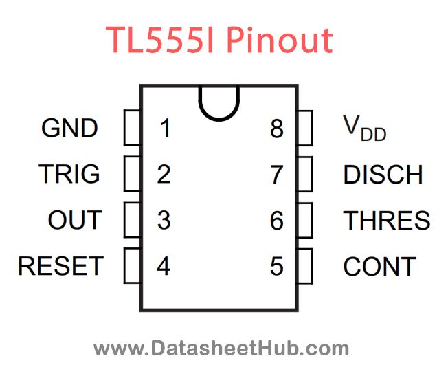
| Pin | Description |
|---|---|
| NAME | |
| CONT | I |
| DISCH | O |
| GND | — |
| NC | — |
| OUT | O |
| RESET | I |
| THRES | I |
| TRIG | I |
| VDD | — |
Absolute maximum ratings
| Parameter | Value | Unit |
|---|---|---|
| Voltage | Min Supply, VDD(2) / Min –0.3 | 18 |
| Input, any input | Min –0.3 / Min VDD | |
| Discharge | Min –0.3 / Min 18 | |
| Current | Min Sink, discharge or output / Min 150 | mA |
| Source, output, IO | Min 15 | |
| Temperature | Min Operating, TA / Min C-suffix | 0 |
| I-suffix | Min –40 / Min 85 | |
| Q-suffix | Min –40 / Min 125 | |
| M-suffix | Min –55 / Min 125 | |
| Case, for 60 seconds | Min FK package / Min –65 | 150 |
| Storage, Tstg | Min –65 / Min 150 |
TL555I applications
- Precision timing
- Pulse generation
- Sequential timing
- Time delay generation
- Pulse width modulation
- Pulse position modulation
- Linear ramp generator
More about TL555I
TL555I Features
- Very low power consumption:
- High output current capability
- Available in Q-temp automotive
TL555I Absolute Maximum Ratings
1) Stresses beyond those listed under Absolute Maximum Ratings may cause permanent damage to the device. These are stress ratings only, which do not imply functional operation of the device at these or any other conditions beyond those indicated under Recommended Operating Conditions. Exposure to absolute-maximum-rated conditions for extended periods may affect device reliability.
2) All voltage values are with respect to network GND.
Pin Definitions
| PIN | I/O | DESCRIPTION | |
| NAME | SOIC, PDIP, SOP, CDIP | ||
| CONT | 5 | I | Controls comparator thresholds. Outputs 2/3 VDD and allows bypass capacitor connection. |
| DISCH | 7 | O | Open collector output to discharge timing capacitor. |
| GND | 1 | — | Ground. |
| NC | — | — | No internal connection. |
| OUT | 3 | O | High current timer output signal. |
| RESET | 4 | I | Active low reset input forces output and discharge low. |
| THRES | 6 | I | End of timing input. THRES > CONT sets output low and discharge low. |
| TRIG | 2 | I | Start of timing input. TRIG < 1/2 CONT sets output high and discharge open. |
| VDD | 8 | — | Power-supply voltage. |
Comments 0
Leave a comment