

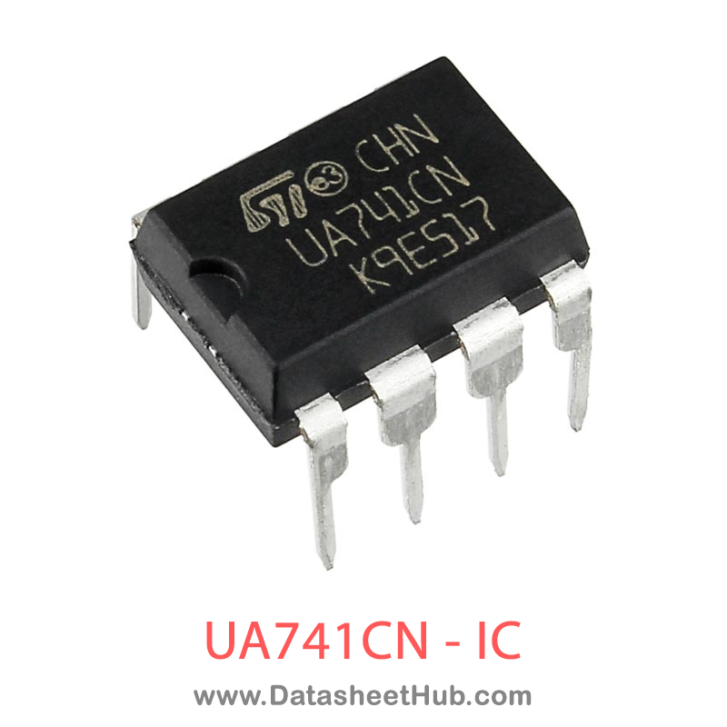
UA741CN Datasheet – Single Operational Amplifier IC
General purpose operational amplifier
Package DIP 8 Pin

UA741CN overview
The UA741 is a high-performance monolithic operational amplifier constructed on a single silicon chip. It is intended for a wide range of analog applications. The high gain and wide range of operating voltages provide superior performances in integrators, summing amplifiers, and general feedback applications. The internal compensation network (6 dB/octave) ensures stability in closed-loop circuits.
| Part Number | UA741CN |
| Function | General purpose operational amplifier |
| Package | DIP 8 Pin |
| Manufacturer | STMicroelectronics |
| Datasheet | Download PDF  |
Datasheet
ua741-datasheet.pdf
UA741CN features
- Large input voltage range
- No latch-up
- High gain
- Short-circuit protection
- No frequency compensation required
- Same pin configuration as the UA709
UA741CN pinout
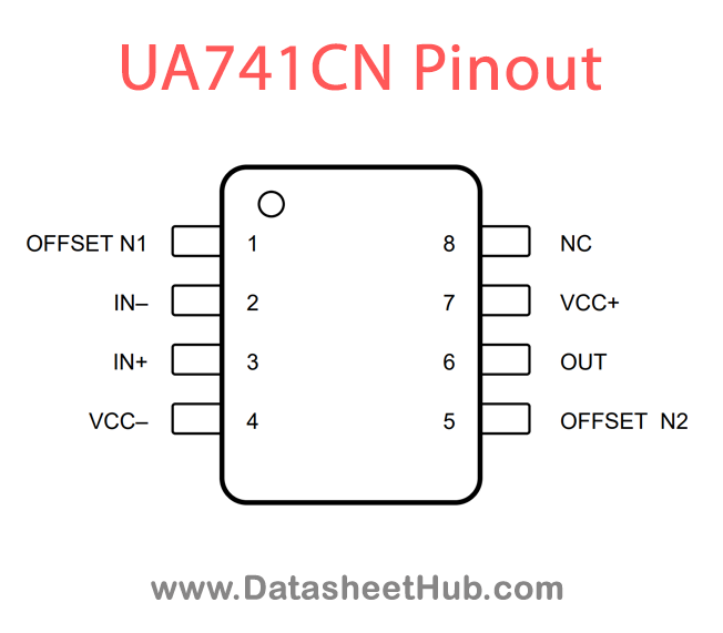
| Pin | Description |
|---|---|
| NAME | |
| IN+ | I |
| IN– | I |
| NC | — |
| OFFSET N1 | I |
| OFFSET N2 | I |
| OUT | O |
| VCC+ | — |
| VCC– | — |
Absolute maximum ratings
| Parameter | Symbol | Value | Unit |
|---|---|---|---|
| Supply voltage | VCC | ±22 | V |
| Differential input voltage | Vid | ±30 | |
| Input voltage | Vi | ±15 | |
| Output short-circuit duration | Infinite | ||
| Thermal resistance junction to ambient DIP8SO8 | Rthja | 85125 | °C/W |
| Thermal resistance junction to caseDIP8SO8 | Rthjc | 4140 | |
| HBM: human body model (1) DIP packageSO package | ESD | 500400 | V |
| 100 | MM: machine model (2) | ||
| 1.5 | CDM: charged device model (3) | kV | |
| Storage temperature range | Tstg | -65 to +150 | °C |
UA741CN applications
- Summing amplifiers
- Voltage followers
- Integrators
- Active filters
- Function generators
- DVDRecordersand Players
- ProAudio Mixers
More about UA741CN
Absolute Maximum Ratings
- Human body model: a 100 pF capacitor is charged to the specified voltage, then discharged through a 1.5kΩ resistor between two pins of the device. This is done for all couples of connected pin combinations while the other pins are floating.
- Machine model: a 200 pF capacitor is charged to the specified voltage, then discharged directly between two pins of the device with no external series resistor (internal resistor < 5 Ω). This is done for all couples of connected pin combinations while the other pins are floating.
- Charged device model: all pins and the package are charged together to the specified voltage and then discharged directly to the ground through only one pin. This is done for all pins.
Pin Definitions
| PIN | I/O | DESCRIPTION | |
| IN+ | 3 | I | Noninverting input |
| IN– | 2 | I | Inverting input |
| NC | 8 | — | No internal connection |
| OFFSET N1 | 1 | I | External input offset voltage adjustment |
| OFFSET N2 | 5 | I | External input offset voltage adjustment |
| VCC+ | 7 | — | Positive supply |
| VCC– | 4 | — | Negative supply |
Comments 0
Leave a comment