

UP7711U8 Datasheet – 2A Ultra Low Dropout Linear Regulator IC

UP7711U8 overview
The UP7711U8 is a 2A Ultra Low Dropout Linear Regulator made by NEC, supplied in an SOP 8 Pin package. The absolute maximum ratings table on this page lists the 9 limits from the manufacturer's datasheet that must not be exceeded. This page brings together the UP7711U8 pinout and maximum ratings, with the full datasheet PDF to preview below or download.
The RT9045 is a simple, cost-effective and high-speed linear regulator designed to generate termination voltage in Double Data Rate (DDR) memory system to comply with the devices requirements. The regulator is capable of actively sinking or sourcing up to 1.8A while regulating an output voltage to within 20mV. The output termination voltage can be tightly regulated to track VDDQ / 2 by two external voltage divider resistors or the desired output voltage can be programmed by externally forcing the REFEN pin voltage. The RT9045 also incorporates a high-speed differential amplifier to provide ultra-fast response in line/load transient. Other features include extremely low initial offset voltage, excellent load regulation, current limiting in bi-directions and on-chip thermal shutdown protection.
Datasheet
UP7711U8 features
- l Ideal for DDR VTT Applications
- Sink and Source Current
- DDRII 1.8A Sink/Source @ VIN = 1.8V
- DDRIII 1.5A Sink/Source @ VIN = 1.5V
- LPDDRIII 1.2A Sink/Source @ VIN = 1.35V
- DDRIV 1.2A Sink/Source @ VIN = 1.2V
- l Integrated Power MOSFETs
- Generate Termination Voltage for DDR Memory Interfaces
- l Stable with Output Ceramic Capacitor
- High Accuracy Output Voltage at Full-Load
- l Output Adjustment by Two External Resistors
- Low External Component Count
- l Shutdown for Suspend to RAM (STR) Functionality with High Impedance Output
- Current Limiting Protection
- l On-Chip Thermal Protection
- RoHS Compliant
UP7711U8 pinout
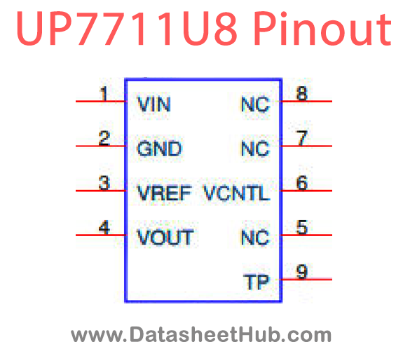
| Name | Description |
|---|---|
| VIN | Input voltage which supplies current to the output pin. Connect this pin to a well-decoupled supply voltage. To prevent the input rail from dropping during large load transient, a large, low ESR capacitor is recommended to use. The capacitor should be placed as close as possible to the VIN pin. |
| GND (Exposed Pad) | Common Ground. The exposed pad must be soldered to a large PCB and connected to GND for maximum power dissipation. |
| VCNTL | VCNTL supplies the internal control circuitry and provides the drive voltage. The driving capability of output current is proportioned to the VCNTL. Connect this pin to 5V bias supply to handle large output current with at least 1mF capacitor from this pin to GND. An important note is that VIN shoul |
| REFEN | Reference voltage input and active low shutdown control pin. Two resistors dividing down the VIN voltage on this pin to create the regulated output voltage. Pulling this pin to ground turns off the device by an open-drain, such as 2N7002, signal N-MOSFET. |
| VOUT | Regulator output. VOUT is regulated to REFEN voltage that is used to terminate the bus resistors. It is capable of sinking and sourcing current while regulating the output rail. To maintain adequate large signal transient response, typical value of 10mF ceramic capacitors are recommended to reduce t |
Absolute maximum ratings
| Parameter | Value |
|---|---|
| Input Voltage, VIN | 0.3V to 6V |
| Control Voltage, VCNTL | 0.3V to 6V |
| Reference Input Voltage, VREFEN | 0.3V to 6V |
| Output Voltage, VOUT | 0.3V to 6V |
| l Power Dissipation, PD @ TA = 25°CSOP-8 (Exposed Pad) | 2.51W |
| l Package Thermal Resistance (Note 2) SOP-8 (Exposed Pad), qJASOP-8 (Exposed Pad), qJC | 39.8°C/W10.1°C/W |
| Junction Temperature | 150°C |
| Lead Temperature (Soldering, 10 sec.) | 260°C |
| l ESD Susceptibility (Note 3) HBM (Human Body Model) MM (Machine Model) | 2kV200V |
UP7711U8 applications
- Desktop PCs, Notebooks, and Workstations
- Graphics Card Memory Termination
- Set Top Boxes, Digital TVs, Printers
- Embedded Systems
- Active Termination Buses
- DDR Memory Systems
Comments 0
Leave a comment