
XL1509 Datasheet – 2A, 40V Buck DC to DC Converter – XLSEMI
2A, 150KHz, 40V, Buck DC to DC Converter

XL1509 overview
The XL1509 is a 2A, 150KHz, 40V, Buck DC to DC Converter made by XLSEMI, supplied in an SOP 8 Pin Type package. The absolute maximum ratings table on this page lists the 10 limits from the manufacturer's datasheet that must not be exceeded. This page brings together the XL1509 pinout and maximum ratings, with the full datasheet PDF to preview below or download.
The XL1509 is a 150 KHz fixed frequency PWM buck (step-down) DC/DC converter, capable of driving a 2A load with high efficiency, low ripple and excellent line and load regulation. Requiring a minimum number of external components, the regulator is simple to use and include internal frequency compensation and a fixed-frequency oscillator. The PWM control circuit is able to adjust the duty ratio linearly from 0 to 100%. An enable function, an over current protection function is built inside. When second current limit function happens, the operation frequency will be reduced from 150KHz to 50KHz. An internal compensation block is built in to minimize external component count.
Datasheet
XL1509 features
- Wide 4.5V to 40V Input Voltage Range
- 3.3V,5V,12V, and adjustable versions
- Output Adjustable from 1.23V to 37V
- Maximum Duty Cycle 100%
- Minimum Drop Out 1.5V
- Fixed 150KHz Switching Frequency
- 2A Constant Output Current Capability
- Internal Optimize Power Transistor
- High efficiency
- Excellent line and load regulation
- TTL shutdown capability
- ON/OFF pin with hysteresis function
- Built in thermal shutdown function
- Built in current limit function
- Built in second current limit function
- Available in SOIC8 package
XL1509 pinout
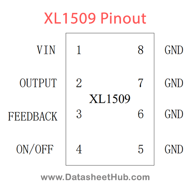
| Pin | Name | Description |
|---|---|---|
| 1 | VIN | Supply Voltage Input Pin. XL1509 operates from a 4.5V to 40V DC voltage. Bypass Vin to GND with a suitably large capacitor to eliminate noise on the input. |
| 2 | OUTPUT | Power Switch Output Pin (SW). Output is the switch node that supplies power to the output. |
| 5~8 | GND | Ground Pin. Care must be taken in layout. This pin should be placed outside of the Schottky Diode to output capacitor ground path to prevent switching current spikes from inducing voltage noise into XL1509. |
| 3 | FEEDBACK | Feedback Pin (FB). Through an external resistor divider network, Feedback senses the output voltage and regulates it. The feedback threshold voltage is 1.23V. |
| 4 | ON/OFF | Enable Pin. Drive ON/OFF pin low to turn on the device, drive it high to turn it off. Floating is default low. |
Absolute maximum ratings
| Parameter | Symbol | Value | Unit |
|---|---|---|---|
| Input Voltage | Vin | -0.3 to 45 | V |
| Feedback Pin Voltage | VFB | -0.3 to Vin | V |
| ON/OFF Pin Voltage | VON/OFF | -0.3 to Vin | V |
| Output Switch Pin Voltage | VOutput | -0.3 to Vin | V |
| Power Dissipation | PD | Internally limited | mW |
| Thermal Resistance (SOIC8) (Junction to Ambient, No Heatsink, Free Air) | RJA | 100 | ºC/W |
| Operating Junction Temperature | TJ | -40 to 125 | ºC |
| Storage Temperature | TSTG | -65 to 150 | ºC |
| Lead Temperature (Soldering, 10 sec) | TLEAD | 260 | ºC |
| ESD (HBM) | 2000 | V |
XL1509 applications
- LCD Monitor and LCD TV
- Digital Photo Frame
- Set-up Box
- ADSL Modem
- Telecom / Networking Equipment
Comments 0
Leave a comment