

74LS112 Dual J-K Negative Edge-triggered Flip-Flop
Package PDIP, SOIC Series 74LS
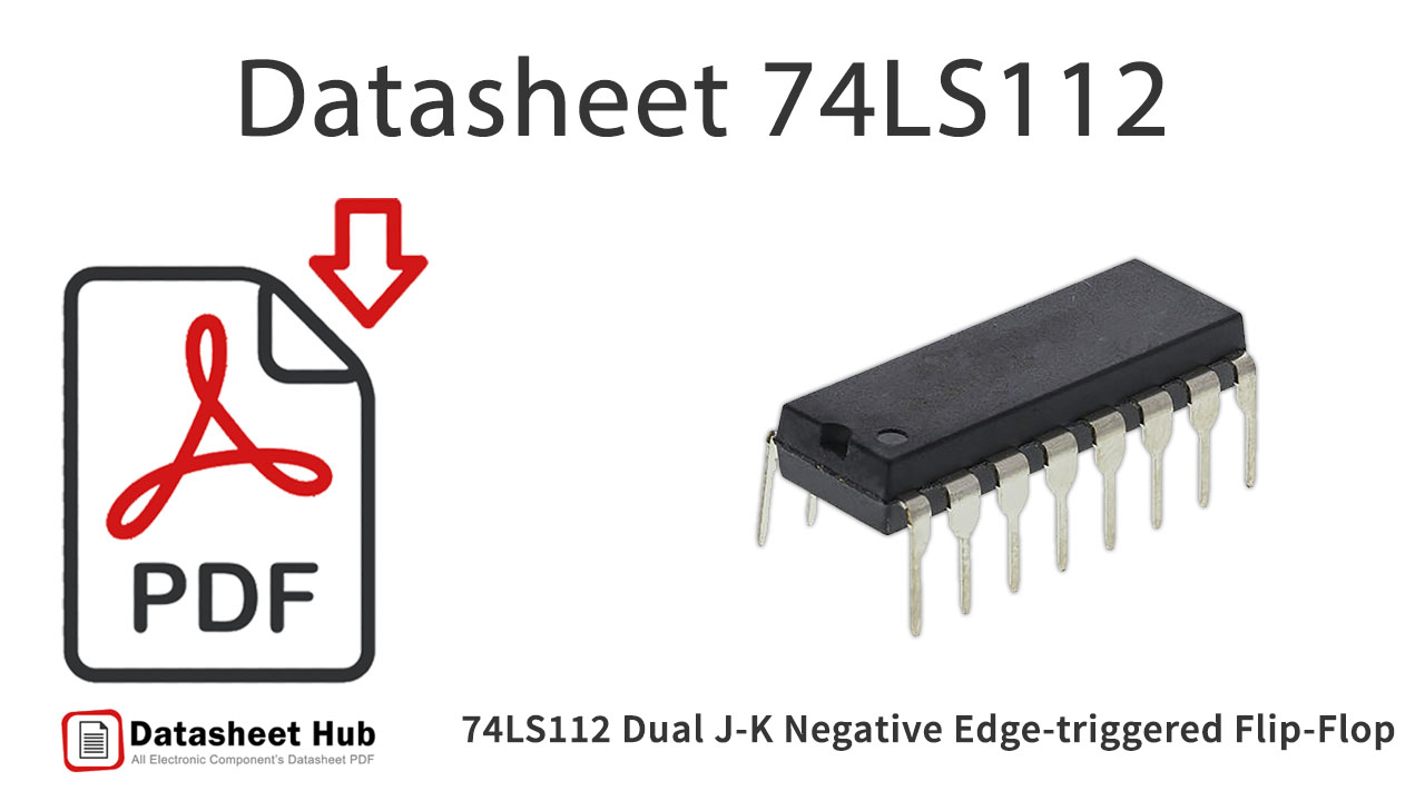
74LS112 overview
The 74LS series of integrated circuits (ICs) was one of the most popular logic families of transistor-transistor logic (TTL) logic chips. 74LS series is a bipolar, low-power Schottky IC. 74LS112 contains two independent J-K negative-edge-triggered flip-flops. A low level at the preset and clear inputs set or resets the outputs regardless of the levels of the other inputs.

Key specifications
Supply Voltage
4.75 - 5.25Vdc
Maximum Clock Frequency
40Mhz
Power Dissipation
2mW/gate @100kHz
Minimum Output Current
8mA
Propagation Delay
10nS
Fan Out (TTL Loads)
20
Datasheet
112.pdf
74LS112 features
- Two Independent JK Negative Edge Triggered Flip-Flops
- Separate Preset and Clear Inputs
- Fast Switching Times
- Operating Temperature up to 70°C
- Standard TTL Switching Voltages
74LS112 pinout

| Pin | Name | Description |
|---|---|---|
| 1 | CP | Clear/Clock Pin |
| 2 | K1 | Data Input Pin K1 |
| 3 | J1 | Data Input Pin J1 |
| 4 | SD | Serial Data Pin |
| 5 | Q1' | Output Active Low Pin Q1' |
| 6 | Q1 | Output Active High Pin Q1 |
| 7 | Q2 | Output Active High Pin Q2 |
| 8 | GND | Ground |
| 9 | Q2' | Output Active Low Pin Q2' |
| 10 | SD | Serial Data Pin |
| 11 | J2 | Data Input Pin J2 |
| 12 | K2 | Data Input Pin K2 |
| 13 | CP | Clear/Clock Pin |
| 14 | CD1 | Digital Clock Pin 1 |
| 15 | CD2 | Digital Clock Pin 2 |
| 16 | VCC | Positive Supply |
74LS112 applications
- Event Detectors
- Data Synchronizers
- Frequency Divider
More about 74LS112
74LS112 Alternative Equivalent
74LS107, 74LS109
Comments 0
Leave a comment