

74LS74 Dual D-Type Flip-Flop
74LS74 overview
The 74LS series of integrated circuits (ICs) was one of the most popular logic families of transistor-transistor logic (TTL) logic chips. 74LS series is a bipolar, low-power Schottky IC. 74LS74 Dual D-Type Flip-Flop contains two independent D-type positive-edge-triggered flip-flops. A low level at the preset or clear inputs sets or resets the outputs regardless of the levels of the other inputs. When preset and clear are inactive (high), data at the D input meeting the setup time requirements are transferred to the outputs on the positive-going edge of the clock pulse. Clock triggering occurs at a voltage level and is not directly related to the rise time of the clock pulse. Following the hold-time interval, data at the D input may be changed without affecting the levels at the outputs.
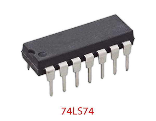
Key specifications
Datasheet
74LS74 features
- Two Independent Negative Edge Triggered JK Flip-Flops
- Standard Pin Arrangement
- Fast Switching Times
- Operating Temperature up to 70°C
- Standard TTL Switching Voltages
74LS74 pinout
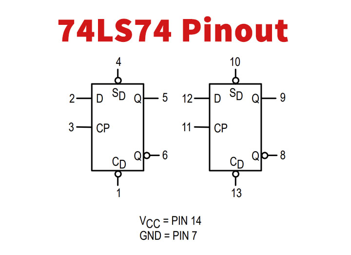
| Pin | Name | Description |
|---|---|---|
| 1 | CD | Clock Pin |
| 2 | D | D Flip Flop Pin |
| 3 | CP | Clear Pin |
| 4 | SD | Serial Data Pin |
| 5 | Q1 | The output logic level Q1 |
| 6 | Q1' | The output logic level Q1' |
| 7 | GND | Ground |
| 8 | Q2' | The output logic level Q2' |
| 9 | Q2 | The output logic level Q2' |
| 10 | SD | Serial Data Pin |
| 11 | CP | Clear Pin |
| 12 | D | D Flip Flop Pin |
| 13 | CD | Clock Pin |
| 14 | VCC | Positive Supply |
74LS74 applications
- Create delay-lines
More about 74LS74
74LS74 Alternative Equivalent
74LS273, 74LS373
Comments 0
Leave a comment