

CD4051 Single 8-channel Multiplexer/Demultiplexer
Package SOIC, SOP, PDIP Series CD4000 (CMOS)
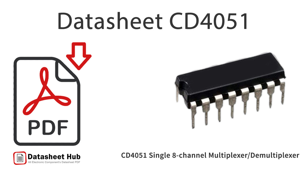
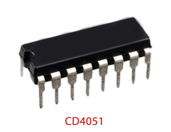
CD4051 overview
CD4051 belongs to the 4000 Series CMOS Logic Family of Integrated Circuits (IC's) constructed with N- and P-channel enhancement mode transistors. CD4051 has a Single 8-channel Multiplexer/Demultiplexer
CD4051 has a supply voltage range of 5V to 20V, which is much higher than any contemporary logic family. It has buffered output which improves transfer characteristics by providing very high gain. All inputs are protected against static discharge with diodes to VDD and VSS.
Datasheet
cd4051.pdf
CD4051 features
- Wide range of digital and analog signal levels: digital 3 – 15V, analog to 15Vp-p
- digital 3 – 15V, analog to 15Vp-p
- Low “ON” resistance: 80Ω (typ.) over entire 15Vp-psignal-input range for VDD − VEE = 15V
- signal-input range for VDD − VEE = 15V
- High “OFF” resistance: channel leakage of ±10 pA (typ.) at VDD − VEE = 10V
- Logic level conversion for digital addressing signals of3 – 15V (VDD − VSS = 3 – 15V) to switch analog signals to 15 Vp-p (VDD − VEE = 15V)
- 3 – 15V (VDD − VSS = 3 – 15V) to switch analog signals to 15 Vp-p (VDD − VEE = 15V)
- Matched switch characteristics: ∆RON = 5Ω (typ.) for VDD − VEE = 15V
- Very low quiescent power dissipation under all digital-control input and supply conditions:1 µ W (typ.) at VDD − VSS = VDD − VEE = 10V
- 1 µ W (typ.) at VDD − VSS = VDD − VEE = 10V
- Binary address decoding on chip
CD4051 pinout
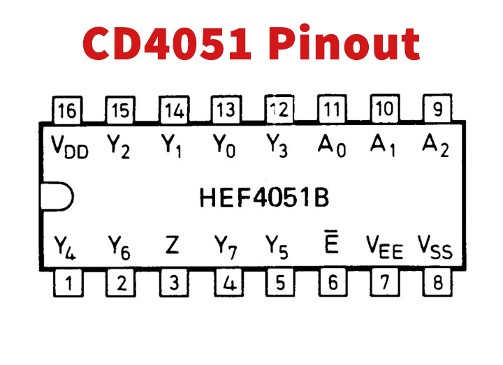
| Pin | Name | Description |
|---|---|---|
| 1 | Y4 | Output 4 Of Multiplexer/Demultiplexer |
| 2 | Y6 | Output 6 Of Multiplexer/Demultiplexer |
| 3 | Z | Common Input/Output Pin |
| 4 | Y7 | Output 7 Of Multiplexer/Demultiplexer |
| 5 | Y5 | Output 5 Of Multiplexer/Demultiplexer |
| 6 | E' | Enable input (active LOW) |
| 7 | VEE | Emitter Voltage |
| 8 | VSS | Supply Voltage |
| 9 | A2 | address input A2 |
| 10 | A1 | address input A1 |
| 11 | A0 | address input A0 |
| 12 | Y3 | Output 3 Of Multiplexer/Demultiplexer |
| 13 | Y0 | Output 0 Of Multiplexer/Demultiplexer |
| 14 | Y1 | Output 1 Of Multiplexer/Demultiplexer |
| 15 | Y2 | Output 2 Of Multiplexer/Demultiplexer |
| 16 | VDD | Drain Voltage |
Absolute maximum ratings
| Parameter | Value |
|---|---|
| DC Supply Voltage Range, (VDD) | -0.5V to +18V |
| Input Voltage Range, All Inputs | -0.5V to VDD +0.5V |
| DC Input Current, Any One Input | ±10mA |
| Storage Temperature Range (TSTG) | -65oC to +150oC |
| Lead Temperature (During Soldering) | +260oC |
CD4051 applications
- Communication System
- Computer Memory
- Telephone Network
- Transmission from the Computer System of a Satellite
- Arithmetic Logic Unit
- Serial to Parallel Converter
CD4051 alternatives and equivalents
- CD4052
- CD4053
More about CD4051
CD4051 Features
- Low “ON” resistance: 80Ω (typ.) over entire 15Vp-p
- Logic level conversion for digital addressing signals of
Absolute Maximum Ratings
- Power Dissipation (PD)
- Dual-In-Line 700 mW
- Small Outline 500 mW
- Lead Temperature (During Soldering): +260oC
- At Distance 1/16 ± 1/32 Inch (1.59mm ± 0.79mm) from case for 10s Maximum
CD4051 Alternative Equivalent
CD4052, CD4053
Comments 0
Leave a comment